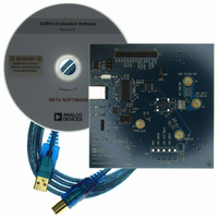
AD9913/PCBZ Analog Devices Inc, AD9913/PCBZ Datasheet
AD9913/PCBZ
Specifications of AD9913/PCBZ


Related parts for AD9913/PCBZ


AD9913/PCBZ Summary of contents
Page 1
FEATURES 250 MSPS internal clock speed 100 MHz analog output Integrated 10-bit DAC 0.058 Hz or better frequency resolution 0.022° phase tuning resolution Programmable modulus in frequency equation Phase noise ≤ –135 dBc per Hz ...
Page 2
AD9913 TABLE OF CONTENTS Features .............................................................................................. 1 Applications ....................................................................................... 1 General Description ......................................................................... 1 Functional Block Diagram .............................................................. 1 Revision History ............................................................................... 2 Specifications ..................................................................................... 3 Electrical Specifications ............................................................... 3 Absolute Maximum Ratings ............................................................ 5 ESD Caution .................................................................................. 5 Equivalent ...
Page 3
SPECIFICATIONS ELECTRICAL SPECIFICATIONS AVDD (1.8 V), DVDD (1.8 V), and DVDD_I/O = 1.8 V ± 5 25°C, R reference clock frequency = 250 MHz with REF_CLK multiplier disabled, unless otherwise noted. Table 1. Parameter REF_CLK INPUT CHARACTERISTICS Frequency ...
Page 4
AD9913 Parameter MISCELLANEOUS TIMING CHARACTERISTICS 1 Wake-Up Time Fast Recovery Mode Full Sleep Mode Reset Pulse Width High DATA LATENCY (PIPELINE DELAY) Frequency, Phase-to-DAC Output Frequency-to-DAC Output Phase-to-DAC Output Delta Tuning Word-to-DAC Output (Linear Sweep) CMOS LOGIC INPUTS Logic 1 ...
Page 5
ABSOLUTE MAXIMUM RATINGS Table 2. Parameter Maximum Junction Temperature AVDD, DVDD Digital Input Voltage Digital Output Current Storage Temperature Operating Temperature Lead Temperature (Soldering, 10 sec) θ JA θ JC EQUIVALENT CIRCUITS INPUT AVOID OVERDRIVING DIGITAL INPUTS. FORWARD BIASING ESD ...
Page 6
AD9913 PIN CONFIGURATION AND FUNCTION DESCRIPTIONS Table 3. Pin Function Descriptions Pin No. Mnemonic I/O Description 1 PS2/ADR5/D5 I/O Multipurpose pin: Profile Select Pin (PS2) in Direct Switch Mode, Parallel Port Address Line (ADR5), and Data Line (D5) to program ...
Page 7
Pin No. Mnemonic I/O Description 26 PWR_DWN_CTL I External Power-Down, Digital Input (Active High). A high level on this pin initiates the currently programmed power-down mode. See the Power-Down Features section for further details. If unused, tie to ground. 27 ...
Page 8
AD9913 TYPICAL PERFORMANCE CHARACTERISTICS 0 −10 −20 −30 −40 −50 −60 −70 −80 −90 −100 FREQUENCY (MHz) Figure 4. Wideband SFDR @ 99.76 MHz f (250 MHz Clock DAC Full-Scale Current, PLL Bypassed) 0 ...
Page 9
SYSTEM CLOCK (MHz) Figure 10. SFDR vs. System Clock Frequency (PLL Bypassed) –100 –110 –120 –130 –140 –150 –160 –170 10 100 1k 10k 100k ...
Page 10
AD9913 −60 −80 VCO 1 −100 VCO 2 −120 −140 −160 100 1k 10k 100k FREQUENCY (MHz) Figure 14. Absolute Phase Noise, VCO1 vs. VCO2 40 DVDD AVDD (PLL) 35 AVDD (CLK) AVDD (DAC) AVDD (DAC CLK ...
Page 11
APPLICATIONS CIRCUITS AD9913 SPLITTER – – – SIDEBAND SELECTION + FILTER – ADC Figure 17. RFID Block Diagram (Only I-Channel of Receiver Shown) INPUT SIGNAL LOW-PASS BAND-PASS FILTER FILTER INPUT ATTENUATOR LOCAL OSCILLATOR AD9913 AS SWEEP GENERATOR ...
Page 12
AD9913 THEORY OF OPERATION DDS CORE The DDS block generates a reference signal (sine or cosine based on the selected DDS sine output bit). The parameters of the reference signal (frequency and phase), are applied to the DDS at its ...
Page 13
AUXILIARY ACCUMULATOR In addition to the phase accumulator of the DDS, the AD9913 has an auxiliary accumulator. This accumulator can be con- figured to support either an automatic sweep of one of the programmable characteristics of the DDS output (frequency ...
Page 14
AD9913 MODES OF OPERATION The AD9913 operates in four modes: • Single tone • Direct switch • Programmable modulus • Linear sweep The modes relate to the data source used to supply the DDS with its signal control parameters: frequency, ...
Page 15
Table 5. Determining the Direction of the Linear Sweep Profile Pins [2:0] or CFR1 Bits [22:20] 1 x00 1 x01 1 x10 1 x11 don’t care. Note that if the part is used in parallel port programming ...
Page 16
AD9913 RAMP-UP MODE (EDGE TRIGGERED NO-DWELL BIT = 0 PS[0] PS[ NO-DWELL BIT = 1 PS[0] PS[1] RAMP-UP MODE (LEVEL TRIGGERED NO-DWELL BIT = 0 PS[0] PS[ NO-DWELL BIT = 1 PS[0] ...
Page 17
BIDIRECTIONAL MODE (EDGE TRIGGERED NO-DWELL BIT = x PS[0] PS[1] BIDIRECTIONAL MODE (LEVEL TRIGGERED NO-DWELL BIT = 0 PS[0] PS[ NO-DWELL BIT = 1 PS[0] PS[1] Figure 24. Display of Bidirectional Ramp Capability Using ...
Page 18
AD9913 CLOCK INPUT (REF_CLK) REF_CLK OVERVIEW The AD9913 supports a number of options for producing the internal SYSCLK signal (that is, the DAC sample clock) via the REF_CLK input pins. The REF_CLK input can be driven directly from a differential ...
Page 19
PLL circuit with an active low signal. The function of CFR2 [ power up or power down the PLL. CFR2 [4] is the PLL LO range bit. When operating the AD9913 ...
Page 20
AD9913 Table 7. PLL Multiplication Factor Configuration CFR2 [13:9] 00000 00001 00010 00011 00100 00101 00110 00111 01000 01001 01010 01011 01100 01101 01110 01111 10000 10001 10010 10011 10100 10101 10110 10111 11000 11001 11010 11011 11100 11101 11110 ...
Page 21
POWER-DOWN FEATURES The AD9913 supports an externally controlled power-down feature as well as software programmable power-down bits consistent with other Analog Devices, Inc. DDS products. The external PWR_DWN_CTL pin determines the power- down scheme. A low on this pin allows ...
Page 22
AD9913 I/O PROGRAMMING SERIAL PROGRAMMING The AD9913 serial port is a flexible, synchronous serial communications port allowing an easy interface to many industry standard microcontrollers and microprocessors. The interface allows read/write access to all registers that configure the AD9913. MSB ...
Page 23
Instruction Byte The instruction byte contains the following information as shown in the instruction byte bit map. Instruction Byte Information Bit Map MSB R —Bit 7 of the instruction ...
Page 24
AD9913 Data Read Operation A typical read operation follows the steps shown in Figure 33. The user supplies PCLK and the parallel address 1. of the register using the address pins (ADR0 through ADR7) for ...
Page 25
REGISTER UPDATE (I/O UPDATE) Functionality of the I/O UPDATE and SYNC_CLK Data from a write sequence is stored in a buffer register (data inactive). An active register exists for every buffer register. The I/O update signal and SYNC_CLK are used ...
Page 26
AD9913 REGISTER MAP AND BIT DESCRIPTIONS REGISTER MAP Note that the highest number found in the Serial Bit Range column for each register in the following tables is the MSB and the lowest number is the LSB for that register. ...
Page 27
Register [Serial Bit Name Range]/ (Serial Parallel MSB Address) Address Bit 7 [7:0]/0x22 Linear Sweep [15:8]/0x23 Ramp Rate Register [23:16]/0x24 (0x08) [31:24]/0x25 Profile 0 [7:0]/0x26 (0x09) [15:8]/0x27 [23:16]/0x28 [31:24]/0x29 [39:32]/0x2A [47:40]/0x2B Open [1:0] Profile 1 [7:0]/0x2C (0x0A) [15:8]/0x2D [23:16]/0x2E [31:24]/0x2F ...
Page 28
AD9913 REGISTER BIT DESCRIPTIONS The serial I/O port registers span an address range (0x00 to 0x10 in hexadecimal notation). This represents a total of 17 registers. However, one of these registers (0x05) is unused, yielding a ...
Page 29
Bit(s) Bit Name 13:12 Destination 11 Auxiliary Accumulator Enable 10 DC Output Active 9 Linear Sweep State Trigger Active 8 Linear Sweep No-Dwell Active 7 External Power-Down Mode 6 Digital Power-Down 5 DAC Power-Down 4 Clock Input Power-Down 3 LOAD ...
Page 30
AD9913 Control Function Register 2 (CFR2) Address 0x01; 2 bytes are assigned to this register. Table 11. Bit Descriptions for CFR2 Bit(s) Bit Name 15 PLL Output Div by 2 14:9 PLL Multiplication Factor 8 Open 7 CMOS Clock Mode ...
Page 31
Linear Sweep Parameter Register Address 0x06, 8 bytes are assigned to this register. This register is only effective if CFR1 [11] or CFR1 [28] are set. See the Auxiliary Accumulator section. Table 15. Bit Descriptions for Linear Sweep Limit Register ...
Page 32
... ORDERING GUIDE 1 Model Temperature Range AD9913BCPZ –40°C to +85°C AD9913BCPZ-REEL7 –40°C to +85°C AD9913/PCBZ RoHS Compliant Part. ©2007–2010 Analog Devices, Inc. All rights reserved. Trademarks and registered trademarks are the property of their respective owners. 5.00 BSC SQ 0.60 MAX 24 0 ...