PDK-N-12864WO-3A DENSITRON, PDK-N-12864WO-3A Datasheet - Page 17
PDK-N-12864WO-3A
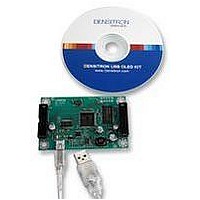
Manufacturer Part Number
PDK-N-12864WO-3A
Description
PMOLED, USB, EVALUATION KIT
Manufacturer
DENSITRON
Type
Evaluation Kitr
Datasheet
1.DD-12864WO-3A.pdf
(27 pages)
Specifications of PDK-N-12864WO-3A
Svhc
No SVHC (18-Jun-2010)
Mcu Supported Families
DD-12864WO-3A
Lead Free Status / RoHS Status
Lead free / RoHS Compliant


5 FUNCTIONAL SPECIFICATION
5.1 COMMANDS
5.2 POWER UP/DOWN SEQUENCE
To protect panel and extend the panel lifetime, the driver IC power up/down routine should
include a delay period between high voltage and low voltage power sources during turn
on/off. It gives the panel enough time to complete the action of charge and discharge
before/after the operation.
5.3 RESET CIRCUIT
Product No.
Copyright ©2010 DENSITRON TECHNOLOGIES plc. All rights reserved. – Proprietary Data
When RES# input is low, the chip is initialized with the following status:
Please refer to the Technical Manual for the SSD1305
1. Display is OFF
2. 132x64 Display mode
3. Normal segment and display data colume and row address mapping (SEG0 mapped to
column address 00H and COM0 mapped to row address 00H)
4. Shift register data clear in serial interface
5. Display start line is set at display RAM address 0
6. Column address counter is set at 0
7. Normal scan direction of the COM outputs
8. Contrast control register is set at 80H
9. Normal display mode (Equivalent to A4h command)
5.2.1 POWER UP SEQUENCE
5.2.2 POWER DOWN SEQUENCE
1. Power up V
2. Send Display off command
3. Initialization
4. Clear Screen
5.Power up V
6. Delay 100ms
(when Vcc is stable)
7. Send Display on command
1. Send Display off command
2. Power down V
3. Delay 100ms
4. Power down V
(When V
completely discharges)
cc
DD-12864WO-3A
CC
reach 0 and panel is
DD
CC
DD
REV. A
V
V
SS
SS
Ground
V
Ground
V
DD
V
V
Display off
Vcc
DD
DD
ON V
CC
CC
ON
V
Display On
CC
Page
off
V
17 /
DD
27
off
Related parts for PDK-N-12864WO-3A
Image
Part Number
Description
Manufacturer
Datasheet
Request
R

Part Number:
Description:
OLED EVAL KIT, 128X32
Manufacturer:
DENSITRON
Datasheet:
Part Number:
Description:
OLED EVAL KIT, 128X64
Manufacturer:
DENSITRON
Datasheet:
Part Number:
Description:
OLED EVAL KIT, 128X64
Manufacturer:
DENSITRON
Datasheet:
Part Number:
Description:
OLED EVAL KIT, 128X64
Manufacturer:
DENSITRON
Datasheet:
Part Number:
Description:
OLED EVAL KIT, 128X64
Manufacturer:
DENSITRON
Datasheet:
Part Number:
Description:
OLED EVAL KIT, 160X128
Manufacturer:
DENSITRON
Datasheet:
Part Number:
Description:
OLED EVAL KIT, 256X64
Manufacturer:
DENSITRON
Datasheet:
Part Number:
Description:
OLED EVAL KIT, 256X64
Manufacturer:
DENSITRON
Datasheet:
Part Number:
Description:
OLED EVAL KIT, 256X64
Manufacturer:
DENSITRON
Datasheet:
Part Number:
Description:
OLED EVAL KIT, 256X64
Manufacturer:
DENSITRON
Datasheet:

Part Number:
Description:
128 x 240 PIXEL INDUSTRIAL TOUCH MONITOR
Manufacturer:
Densitron Corporation
Part Number:
Description:
64 x 240 PIXEL INDUSTRIAL TOUCH MONITOR
Manufacturer:
Densitron Corporation
Part Number:
Description:
320 x 240 PIXEL INDUSTRIAL TOUCH MONITOR
Manufacturer:
Densitron Corporation
Part Number:
Description:
320 x 240 PIXEL INDUSTRIAL TOUCH MONITOR
Manufacturer:
Densitron Corporation
Part Number:
Description:
132 Seg / 65 Com Driver & Controller For Stn Lcd
Manufacturer:
Densitron Corporation
Datasheet: