PDK-N-12864WO-3A DENSITRON, PDK-N-12864WO-3A Datasheet - Page 9
PDK-N-12864WO-3A
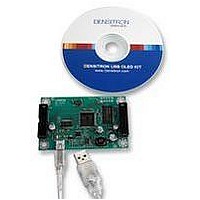
Manufacturer Part Number
PDK-N-12864WO-3A
Description
PMOLED, USB, EVALUATION KIT
Manufacturer
DENSITRON
Type
Evaluation Kitr
Datasheet
1.DD-12864WO-3A.pdf
(27 pages)
Specifications of PDK-N-12864WO-3A
Svhc
No SVHC (18-Jun-2010)
Mcu Supported Families
DD-12864WO-3A
Lead Free Status / RoHS Status
Lead free / RoHS Compliant


3.3 INTERFACE PIN ASSIGNMENT
No.
10
11
9
1
2
3
4
5
6
7
8
Product No.
Copyright ©2010 DENSITRON TECHNOLOGIES plc. All rights reserved. – Proprietary Data
N.C.(GND)
Symbol
RES#
VLSS
R/W#
D/C#
VDD
VSS
N.C.
BS1
BS2
CS#
DD-12864WO-3A
Reserved Pin (Supporting Pin)
The supporting pin can reduce the influence from stress on the function
pins. These pin must be connected to external ground.
Ground of Analog Circuit
This is an analog ground pin. It should be connected to VSS externally
Ground of Logic circuit
This is a ground pin. It also acts as a reference for the logic pins, It must
be connected to external ground.
Reserved Pin
The N.C. pin between function pins is reserved for compatible and
flexible design.
Power Supply for Logic Circuit
This is a voltage supply pin. It must be connected to external source.
Communicating Protocol Select
These pins are MCU interface selection input. See the following table:
Chip Select
This pin is the chip select input. The chip is enabled for MCU
communication only when CS# is pulled low.
Power Reset for Controller and Driver
This pin is reset signal input. When the pin is low, initialization of the chip
is executed.
Data/Command Control
This pin is Data/Command control pin. When the pin is pulled high, the
input at D7~D0 is treated as display data. When the pin is pulled low, the
input at D7~D0 will be transferred to the command register. For detail
relationship to MCU interface signals, please refer to the Timing
Characteristics Diagrams.
When the pin is pulled high and serial interface mode is selected, the
data at SDIN is treated as data. When it is pulled low, the data at SDIN
will be transferred to the command register. In I2C mode, this pin acts as
SA0 for slave address selection.
Read/Write Select or Write
This pin is MCU interface input. When interfacing to a 68XX-series
microprocessor, this pin will be used as Read/Write (R/W#) selection
input. Pull this pin to “High” for read mode and pull it “Low” for write
mode.
When 80XX interface mode is selected, this pin will be the Write (WR#)
input. Data write operation is initiated when this pin is pulled low and the
CS# is pulled low.
REV. A
Function
Page
9 /
27
Related parts for PDK-N-12864WO-3A
Image
Part Number
Description
Manufacturer
Datasheet
Request
R

Part Number:
Description:
OLED EVAL KIT, 128X32
Manufacturer:
DENSITRON
Datasheet:
Part Number:
Description:
OLED EVAL KIT, 128X64
Manufacturer:
DENSITRON
Datasheet:
Part Number:
Description:
OLED EVAL KIT, 128X64
Manufacturer:
DENSITRON
Datasheet:
Part Number:
Description:
OLED EVAL KIT, 128X64
Manufacturer:
DENSITRON
Datasheet:
Part Number:
Description:
OLED EVAL KIT, 128X64
Manufacturer:
DENSITRON
Datasheet:
Part Number:
Description:
OLED EVAL KIT, 160X128
Manufacturer:
DENSITRON
Datasheet:
Part Number:
Description:
OLED EVAL KIT, 256X64
Manufacturer:
DENSITRON
Datasheet:
Part Number:
Description:
OLED EVAL KIT, 256X64
Manufacturer:
DENSITRON
Datasheet:
Part Number:
Description:
OLED EVAL KIT, 256X64
Manufacturer:
DENSITRON
Datasheet:
Part Number:
Description:
OLED EVAL KIT, 256X64
Manufacturer:
DENSITRON
Datasheet:

Part Number:
Description:
128 x 240 PIXEL INDUSTRIAL TOUCH MONITOR
Manufacturer:
Densitron Corporation
Part Number:
Description:
64 x 240 PIXEL INDUSTRIAL TOUCH MONITOR
Manufacturer:
Densitron Corporation
Part Number:
Description:
320 x 240 PIXEL INDUSTRIAL TOUCH MONITOR
Manufacturer:
Densitron Corporation
Part Number:
Description:
320 x 240 PIXEL INDUSTRIAL TOUCH MONITOR
Manufacturer:
Densitron Corporation
Part Number:
Description:
132 Seg / 65 Com Driver & Controller For Stn Lcd
Manufacturer:
Densitron Corporation
Datasheet: