CDB3318 Cirrus Logic Inc, CDB3318 Datasheet - Page 27
CDB3318
Manufacturer Part Number
CDB3318
Description
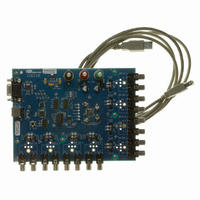
Eval Bd - 8-channel Digital Vol Cntrl
Manufacturer
Cirrus Logic Inc
Specifications of CDB3318
Main Purpose
Audio, Volume Control
Embedded
No
Utilized Ic / Part
CS3318
Primary Attributes
8 Single-Ended Analog Inputs and Outputs, USB or RS232 Interface
Secondary Attributes
Graphical User Interface
Description/function
Audio DSPs
Operating Supply Voltage
8 V to 9 V
Product
Audio Modules
Lead Free Status / RoHS Status
Contains lead / RoHS non-compliant
For Use With/related Products
CS3310
Lead Free Status / RoHS Status
Contains lead / RoHS non-compliant, Contains lead / RoHS non-compliant
Other names
598-1497


DS693F1
5.9
5.9.1
I²C/SPI Serial Control Formats
The control port is used to access the internal registers of the CS3318
and I²C, with the CS3318 acting as a slave device. SPI Mode is selected if there is a high-to-low transition
on the CS pin after the RESET pin has been brought high. I²C Mode is selected by connecting the CS pin
to VD or DGND.
SDA
I²C Mode
In I²C Mode, SDA is a bidirectional data line. Data is clocked into and out of the CS3318 by the clock,
SCL. The AD0 pin sets the least significant bit of the default chip address and must be connected to VD
or DGND. The AD0 pin is read upon the release of the RESET signal (a low-to-high transition), and its
value (‘0’ when connected to DGND, ‘1’ when connected to VD) is reflected in the LSB of the chip address
in the Individual, Group 1, and Group 2 Chip Address registers.
in I²C Mode.
The signal timings for a read and write cycle are shown in
defined as a falling transition of SDA while the clock is high. A Stop condition is a rising transition while
the clock is high. All other transitions of SDA occur while the clock is low.
The first byte sent to the CS3318 after a Start condition consists of a 7-bit chip address field and a R/W
bit (high for a read, low for a write). To communicate with a CS3318, the chip address field should match
either the Individual, Group 1, or Group 2 device address as set by their respective control port registers.
The eighth bit of the address is the R/W bit. If the read/write bit is set high (indicating a read operation)
and the preceding 7 bits do not match its Individual address, the CS3318 will ignore all traffic on the I²C
bus until a Stop and Start condition occurs.
If the operation is a write, the next byte is the Memory Address Pointer (MAP) which selects the register
to be read or written. If the operation is a read, the contents of the register pointed to by the MAP will be
output.
There is a MAP auto-increment capability, enabled by the INCR bit (the MSB of the MAP byte). If INCR
is ‘0’, the MAP will stay constant for successive read or writes. If INCR is ‘1’, the MAP will automatically
increment after each byte is written, allowing block writes of successive registers. Each byte is separated
by an acknowledge (ACK) bit. The ACK bit is output from the CS3318 after each input byte is read and is
input to the CS3318 from the microcontroller after each transmitted byte.
SCL
START
MSB
0
CHIP ADDRESS (WRITE)
1
Chip Address
2
3
4
5
AD0 Connection
LSB
6
Figure 12. Control Port Timing, I²C Write
Table 4. I²C Mode Default Chip Address
7
0
DGND
ACK
8
VD
INCR
9
10 11
6
MAP BYTE
5
12
4
13 14 15
3
Default Chip Address
2
1
16 17 18
0
ACK
1000000b
1000001b
7
Figure 12
19
6
DATA
Table 4
24 25
1
0
ACK
.
26
The control port has 2 modes: SPI
and
27 28
shows the default chip addresses
7
DATA +1
Figure
6
1
0
13. A Start condition is
7
DATA +n
6
1
0
CS3318
ACK
STOP
27
Related parts for CDB3318
Image
Part Number
Description
Manufacturer
Datasheet
Request
R

Part Number:
Description:
Development Kit
Manufacturer:
Cirrus Logic Inc
Datasheet:
Part Number:
Description:
Development Kit
Manufacturer:
Cirrus Logic Inc
Datasheet:


Part Number:
Description:
High-efficiency PFC + Fluorescent Lamp Driver Reference Design
Manufacturer:
Cirrus Logic Inc
Datasheet:
Part Number:
Description:
Development Kit
Manufacturer:
Cirrus Logic Inc
Datasheet:
Part Number:
Description:
Development Kit
Manufacturer:
Cirrus Logic Inc
Datasheet:

Part Number:
Description:
Development Kit
Manufacturer:
Cirrus Logic Inc
Datasheet:
Part Number:
Description:
Development Kit
Manufacturer:
Cirrus Logic Inc
Datasheet:
Part Number:
Description:
Development Kit
Manufacturer:
Cirrus Logic Inc
Datasheet:
Part Number:
Description:
Development Kit
Manufacturer:
Cirrus Logic Inc
Datasheet:

Part Number:
Description:
EVALUATION BOARD FOR CS8427
Manufacturer:
Cirrus Logic Inc
Datasheet:

Part Number:
Description:
BOARD EVAL FOR CS8416 RCVR
Manufacturer:
Cirrus Logic Inc
Datasheet:

Part Number:
Description:
EVALUATION BOARD FOR CS8420
Manufacturer:
Cirrus Logic Inc
Datasheet:

Part Number:
Description:
KIT DEVELOPMENT EP9315 ARM9
Manufacturer:
Cirrus Logic Inc
Datasheet:

Part Number:
Description:
KIT DEVELOPMENT EP9302 ARM9
Manufacturer:
Cirrus Logic Inc
Datasheet: