LK520D3LZ19 Sharp Microelectronics, LK520D3LZ19 Datasheet
LK520D3LZ19
Specifications of LK520D3LZ19


Related parts for LK520D3LZ19


LK520D3LZ19 Summary of contents
Page 1
... P S RODUCT PECIFICATIONS LK520D3LZ19 TFT-LCD Module Spec. Issue Date: October 11, 2006 No: LD-18952 AVC Liquid Crystal Displays Group ...
Page 2
... TECHNICAL TFT - LCD module LK520D3LZ19 MODEL No. The technical literature is subject to change without notice. So, please contact SHARP or its representative before designing your product based on this literature. DEVELOPMENT DEPT Ⅱ DEVELOPMENT CENTER AVC LIQUID CRYSTAL DISPLAY GROUP SHARP CORPORATION No. DATE LITERATURE FOR LD-18952 ...
Page 3
... RECORDS OF REVISION LK520D3LZ19 REVISED SPEC No. DATE No. LD-18952 OCT. 11.2006 PAGE SUMMARY - - NOTE - 1st. Issue ...
Page 4
... Application This technical literature applies to the color 52.0” TFT-LCD module LK520D3LZ19. * These technical literature sheets are proprietary products of SHARP CORPORATION (“SHARP”) and include materials protected under copyright of SHARP. Do not reproduce or cause any third party to reproduce them in any form or by any means, electronic or mechanical, for any purpose, in whole or in part, without the express written permission of SHARP ...
Page 5
Mechanical Specifications Parameter Display size Active area Pixel Format Pixel pitch Pixel configuration Display mode Unit Outline Dimensions (*1) Mass Surface treatment (*1) Outline dimensions are shown in Fig.1 4. Input Terminals 4-1. Block Diagram Input Signal AINO+,AINO-,AIN1+,AIN1-, AIN2+,AIN2-,AIN3+,AIN3-, ...
Page 6
TFT panel driving (Shown in Fig.1) CN1 (Interface signals) Using connector : FI-RE41S-VF (Japan Aviation Electronics Industry, Ltd.) Mating connector : FI-RE41HL (Japan Aviation Electronics Industry, Ltd.) Mating LVDS transmitter : THC63LVDM83R (THine Electronics, Inc.) or equivalent device Pin ...
Page 7
CN2(+12V DC power supply) Using connector : BM20B-SHLDS-G-TFT ( J.S.T. Mfg Co.,Ltd. ) Mating connector : SHLDP-20V-S-1 (J.S.T. Mfg Co.,Ltd.) Pin No. Symbol 1 Vcc 2 Vcc 3 Vcc 4 Vcc 5 Vcc 6 GND 7 GND 8 GND 9 ...
Page 8
Frame side) Port A 8 AR0 ∼ AR7 8 AG0 ∼ AG7 8 AB0 ∼ AB7 ENAB_A Controller CLKA Port B 8 BR0 ∼ BR7 8 BG0 ∼ BG7 8 BB0 ∼ BB7 ENAB_B CLKB Transmitter: ...
Page 9
Transmitter =L(GND) Data R0(LSB) TA0 R1 TA1 R2 TA2 R3 TA3 R4 TA4 R5 TA5 G0(LSB) TA6 G1 TB0 G2 TB1 G3 TB2 G4 TB3 G5 TB4 B0(LSB) TB5 B1 TB6 B2 TC0 B3 TC1 B4 TC2 B5 ...
Page 10
High (3.3V) or OPEN> ACK+,BCK+ ACK-,BCK- AIN0+,BIN0 AIN0-,BIN0- AIN1+,BIN1 AIN1-,BIN1- AIN2+,BIN2 AIN2-,BIN2- AIN3+,BIN3 AIN3-,BIN3- DE: Display Enable NA: Not Available <SELLVDS= Low(GND)> ACK+,BCK+ ACK-,BCK- AIN0+,BIN0 AIN0-,BIN0- AIN1+,BIN1 ...
Page 11
Display reversal function Normal (Default) R (GND) U/D: L (GND) CN1 Vertical reverse image R (GND) U/D: H (3.3V) CN1 [Note 3] O/S control Symbol 50Hz/60Hz Frame frequency setting 1:60Hz, 0:50Hz [Note 4] O/S ...
Page 12
Backlight driving CN3 (Inverter control and +24V DC power supply) Using connector: S14B-PH-K-SB(LF) (J.S.T. Mfg Co.,Ltd.) Mating connector: PHR-14 (J.S.T. Mfg Co.,Ltd.) Pin No. Symbol 1 V INV 2 V INV 3 V INV 4 V INV 5 V ...
Page 13
The back light system characteristics The back light system is direct type with 24 CCFTs (Cold Cathode Fluorescent Tube). The characteristics of the lamp are shown in the following table. The value mentioned below is at the case of ...
Page 14
Input voltage sequences 0 < t1 ≦ 10ms 10ms < t2 ≦ 20ms 10ms < t3 ≦ < t4 ≦ 1ms t5 ≧ 500ms t6 ≧ ≧ 500ms *Please input data signals after clock ...
Page 15
Inverter driving for back light The back light system is direct type with 24 CCFTs (Cold Cathode Fluorescent Tube). Parameter Symbol Current 1 I INV1 + 24V Current 2 I INV2 Supply voltage V INV Permissible input ripple V ...
Page 16
Timing characteristics of input signals 7-1. Timing characteristics Timing diagrams of input signal are shown in Fig.2. Item DCLK Frequency DE (Data Enable) Horizontal total Horizontal valid Horizontal Vertical total Vertical valid 【Note】1) When vertical period is very long, ...
Page 17
Input data signal and display position on the screen (1・1) (1・2) 1・1 1・2 1・3 2・1 2・2 3・1 1080・1 Display position of Data (V,H) 1・1920 LD- 18952-14 1080・1920 ...
Page 18
Input Signal, Basic Display Colors and Gray Scale of Each Color Colors & Gray Gray scale Scale − Black − Blue − Green ...
Page 19
Optical characteristics Parameter θ11,12 Vertical Viewing angle range θ21,22 Horizontal Contrast ratio Response time White Red Chromaticity Green Blue Luminance of white Luminance uniformity Measurement condition : Set the value of V *The measurement shall be executed 60 minutes ...
Page 20
The contrast ratio is defined as the following. Contrast Ratio [Note 3]Definition of response time The response time (τd and τr) is defined as the ...
Page 21
Definition of white uniformity ; White uniformity is defined as the following with five measurements. (A∼E) Maximum luminance of five points (brightness) δ = W Minimum luminance of five points (brightness) 10. Handling Precautions of the module a) ...
Page 22
The module has some printed circuit boards (PCBs) and lamp cables on the back side, take care to keep them form any stress or pressure when handling or installing the module; otherwise some of electronic parts on the PCBs ...
Page 23
Reliability test item No. Test item High temperature storage test 1 Low temperature storage test 2 High temperature and high 3 humidity operation test High temperature operation 4 test Low temperature operation test Ta=0℃ 5 Vibration test (non-operation) 6 ...
Page 24
Others 1)Lot No. Label ; TBD 2) Packing Label TBD 3) Adjusting volume have been set optimally before shipment not change any adjusted value. If adjusted value is changed, the specification may not be satisfied. 4) Disassembling ...
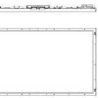
Page 25
Fig.1 OUTLINE DIMENSIONS LD-18952-22 ...
Page 26
... ALL EXPRESS AND IMPLIED WARRANTIES, INCLUDING THE WARRANTIES OF MERCHANTABILITY, FITNESS FOR USE AND FITNESS FOR A PARTICULAR PURPOSE, ARE SPECIFICALLY EXCLUDED event will SHARP be liable any way responsible, for any incidental or consequential economic or property damage. NORTH AMERICA SHARP Microelectronics of the Americas 5700 NW Pacific Rim Blvd. Camas, WA 98607, U.S.A. Phone: (1) 360-834-2500 ...