HCPL2611 Fairchild Semiconductor, HCPL2611 Datasheet - Page 2
HCPL2611
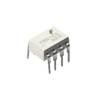
Manufacturer Part Number
HCPL2611
Description
High Speed Optocouplers DIP 8 HS LOGIC GATE
Manufacturer
Fairchild Semiconductor
Datasheet
1.HCPL2611.pdf
(12 pages)
Specifications of HCPL2611
Isolation Voltage
2500 Vrms
Maximum Continuous Output Current
50 mA
Maximum Fall Time
0.012 us
Maximum Forward Diode Current
50 mA
Maximum Rise Time
50 ns
Output Device
Logic Gate Photo IC
Configuration
1 Channel
Maximum Baud Rate
10 Mbps
Maximum Forward Diode Voltage
1.75 V
Maximum Reverse Diode Voltage
5 V
Maximum Power Dissipation
100 mW
Maximum Operating Temperature
+ 85 C
Minimum Operating Temperature
- 40 C
Package / Case
PDIP-B
Number Of Elements
1
Input Type
DC
Output Type
Open Collector
Baud Rate
10Mbps
Forward Voltage
1.75V
Forward Current
50mA
Output Current
50mA
Package Type
PDIP-B
Operating Temp Range
-40C to 85C
Power Dissipation
100mW
Propagation Delay Time
75ns
Pin Count
8
Mounting
Through Hole
Reverse Breakdown Voltage
5V
Operating Temperature Classification
Industrial
Lead Free Status / RoHS Status
Lead free / RoHS Compliant
Other names
HCPL2611_NL
Available stocks
Company
Part Number
Manufacturer
Quantity
Price
Company:

Part Number:
HCPL2611
Manufacturer:
Fairchild Optoelectronics Grou
Quantity:
1 976
Part Number:
HCPL2611
Manufacturer:
FAIRCHILD/仙童
Quantity:
20 000
Company:
Part Number:
HCPL2611020
Manufacturer:
AVAGO
Quantity:
4 766
Company:
Part Number:
HCPL2611300E
Manufacturer:
AVAGO
Quantity:
4 064
Company:
Part Number:
HCPL2611320E
Manufacturer:
AVAGO
Quantity:
5 838
Part Number:
HCPL2611SD
Manufacturer:
FAIRCHILD/仙童
Quantity:
20 000


©2005 Fairchild Semiconductor Corporation
6N137, HCPL2601, HCPL2611, HCPL2630, HCPL2631 Rev. 1.0.8
Absolute Maximum Ratings
Stresses exceeding the absolute maximum ratings may damage the device. The device may not function or be
operable above the recommended operating conditions and stressing the parts to these levels is not recommended.
In addition, extended exposure to stresses above the recommended operating conditions may affect device reliability.
The absolute maximum ratings are stress ratings only.
*For peak soldering reflow, please refer to the Reflow Profile on page 11.
Recommended Operating Conditions
The Recommended Operating Conditions table defines the conditions for actual device operation. Recommended
operating conditions are specified to ensure optimal performance to the datasheet specifications. Fairchild does not
recommend exceeding them or designing to absolute maximum ratings.
*6.3mA is a guard banded value which allows for at least 20% CTR degradation. Initial input current threshold value
is 5.0mA or less.
EMITTER
DETECTOR
(1 minute max)
Symbol
Symbol
T
T
T
V
V
V
V
I
V
V
P
I
OPR
V
T
STG
SOL
P
I
I
FH
N
FL
CC
CC
EH
O
EL
F
A
O
O
E
R
I
Storage Temperature
Operating Temperature
Lead Solder Temperature (for wave soldering only)*
DC/Average Forward
Input Current
Enable Input Voltage Not to Exceed
V
Reverse Input Voltage
Power Dissipation
Supply Voltage
Output Current
Output Voltage
Collector Output
Power Dissipation
Input Current, Low Level
Input Current, High Level
Supply Voltage, Output
Enable Voltage, Low Level
Enable Voltage, High Level
Low Level Supply Current
Fan Out (TTL load)
CC
by more than 500mV
Parameter
(T
A
= 25°C unless otherwise specified)
Parameter
Single Channel
Dual Channel (Each Channel)
Single Channel
Each Channel
Single Channel
Dual Channel (Each Channel)
Single Channel
Dual Channel (Each Channel)
Each Channel
Single Channel
Dual Channel (Each Channel)
2
Min.
*6.3
-40
4.5
2.0
0
0
Max.
V
250
+85
5.5
0.8
260 for 10 sec
15
CC
8
-55 to +125
-40 to +85
Value
100
5.5
5.0
7.0
7.0
50
30
45
50
50
85
60
www.fairchildsemi.com
Units
mA
µA
°C
V
V
V
Units
mW
mW
mA
mA
°C
°C
°C
V
V
V
V
Related parts for HCPL2611
Image
Part Number
Description
Manufacturer
Datasheet
Request
R

Part Number:
Description:
Fairchild Semiconductor [IGBT MODULE]
Manufacturer:
Fairchild Semiconductor
Datasheet:

Part Number:
Description:
Discrete Semiconductor Modules
Manufacturer:
Fairchild Semiconductor
Part Number:
Description:
Discrete Semiconductor Modules
Manufacturer:
Fairchild Semiconductor
Part Number:
Description:
This N-Channel MOSFET is produced using Fairchild Semiconductor’s advanced Power Trench® process
Manufacturer:
Fairchild Semiconductor
Datasheet:
Part Number:
Description:
This N-Channel MOSFET is produced using Fairchild Semiconductor’s advanced Power Trench® process
Manufacturer:
Fairchild Semiconductor
Datasheet:
Part Number:
Description:
This N-Channel MOSFET is produced using Fairchild Semiconductor’s advanced PowerTrench® process
Manufacturer:
Fairchild Semiconductor
Datasheet:
Part Number:
Description:
This N-Channel MOSFET is produced using Fairchild Semiconductor’s advanced PowerTrench® process
Manufacturer:
Fairchild Semiconductor
Datasheet:
Part Number:
Description:
This N-Channel MOSFET is produced using Fairchild Semiconductor’s advanced Power Trench® process
Manufacturer:
Fairchild Semiconductor
Datasheet:
Part Number:
Description:
This N-Channel logic Level MOSFETs are produced using Fairchild Semiconductor‘s advanced Power Trench® process that has been special tailored to minimize the on-state resistance and yet maintain superior switching performance
Manufacturer:
Fairchild Semiconductor
Datasheet:
Part Number:
Description:
This N-Channel MOSFET is produced using Fairchild Semiconductor’s advanced Power Trench® process
Manufacturer:
Fairchild Semiconductor
Datasheet:
Part Number:
Description:
This N-Channel SyncFET™ is produced using Fairchild Semiconductor’s advanced PowerTrench® process
Manufacturer:
Fairchild Semiconductor
Datasheet:
Part Number:
Description:
This N-Channel SyncFET™ is produced using Fairchild Semiconductor’s advanced PowerTrench® process
Manufacturer:
Fairchild Semiconductor
Datasheet:
Part Number:
Description:
This N-Channel SyncFET™ is produced using Fairchild Semiconductor’s advanced PowerTrench® process
Manufacturer:
Fairchild Semiconductor
Datasheet:
Part Number:
Description:
This N-Channel logic Level MOSFETs are produced using Fairchild Semiconductor‘s advanced Power Trench® process that has been special tailored to minimize the on-state resistance and yet maintain superior switching performance
Manufacturer:
Fairchild Semiconductor
Datasheet:
Part Number:
Description:
This N-Channel MOSFET is produced using Fairchild Semiconductor’s advanced Power Trench® process that has been especially tailored to minimize the on-state resistance and yet maintain superior switching performance
Manufacturer:
Fairchild Semiconductor
Datasheet: