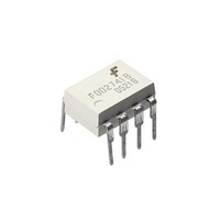
HCPL4502_Q Fairchild Semiconductor, HCPL4502_Q Datasheet - Page 5

HCPL4502_Q
Manufacturer Part Number
HCPL4502_Q
Description
High Speed Optocouplers 1Mbit/s 1Ch Optocoup Transistor Hi Speed
Manufacturer
Fairchild Semiconductor
Datasheet
1.6N135.pdf
(12 pages)
Specifications of HCPL4502_Q
Input Type
DC
Isolation Voltage
2500 Vrms
Maximum Fall Time
0.8 us
Maximum Rise Time
0.8 us
Output Device
Phototransistor
Configuration
1 Channel
Current Transfer Ratio
27 %
Maximum Baud Rate
1 MBps
Maximum Forward Diode Voltage
1.7 V
Maximum Reverse Diode Voltage
5 V
Maximum Input Diode Current
25 mA
Maximum Power Dissipation
100 mW
Maximum Operating Temperature
+ 100 C
Minimum Operating Temperature
- 55 C
Package / Case
PDIP-8
Lead Free Status / RoHS Status
Lead free / RoHS Compliant
©2005 Fairchild Semiconductor Corporation
6N135, 6N136, HCPL2503, HCPL4502, HCPL2530, HCPL2531 Rev. 1.0.7
Electrical Characteristics
Switching Characteristics
** All Typicals at T
Notes:
6. The 4.1k load represents 1 LSTTL unit load of 0.36mA and 6.1k pull-up resistor.
7. The 1.9k load represents 1 TTL unit load of 1.6mA and 5.6k pull-up resistor.
8. Common mode transient immunity in logic high level is the maximum tolerable (positive) dV
Symbol Parameter
|CM
|CM
T
T
of the common mode pulse signal V
Common mode transient immunity in logic low level is the maximum tolerable (negative) dV
of the common mode pulse signal, V
PLH
PHL
H
L
|
|
Propagation Delay
Time to Logic LOW
Propagation Delay
Time to Logic HIGH
Common Mode
Transient
Immunity at
Logic High
Common Mode
Transient
Immunity at
Logic Low
A
= 25°C
(V
CC
T
I
R
T
R
R
T
I
R
T
R
R
I
R
I
R
I
R
I
R
F
F
F
F
F
F
(Continued) (T
= 5V)
A
A
A
A
L
L
L
L
L
L
L
L
L
L
= 16mA
= 16mA
= 0mA, V
= 0mA, V
= 16mA, V
= 16mA, V
= 25°C, R
= 25°C
= 25°C, (R
= 25°C
= 1.9k , I
= 4.1k , I
= 1.9k , I
= 1.9k , I
= 4.1k , I
= 1.9k , I
= 4.1k , T
= 1.9k , T
= 4.1k , T
= 1.9k
CM
CM
, to assure that the output will remain in a logic high state (i.e., V
Test Conditions
, to assure that the output will remain in a logic low state (i.e., V
(7)
(6)
(6)
(8)
CM
CM
L
(Fig. 7)
CM
CM
(Fig. 7)
F
F
F
(Fig. 7)
F
F
F
L
A
A
A
(Fig. 8)
= 4.1k ,
= 16mA,
= 16mA
= 16mA
= 16mA
= 16mA
= 16mA
= 10V
= 10V
= 4.1k ,
A
= 25°C
= 25°C
= 25°C
= 10 V
= 10 V
= 0 to 70°C unless otherwise specified)
P-P
P-P
(8)
(8)
(8)
(6)
(7)
(7)
(6)
(7)
5
P-P
P-P
,
,
(Fig. 8)
(Fig. 8)
(Fig. 8)
(Fig. 7)
(Fig. 7)
(Fig. 7)
(Fig. 7)
(Fig. 7)
,
,
HCPL2530
HCPL4502
HCPL2503
HCPL2531
HCPL2530
HCPL4502
HCPL2503
HCPL2531
HCPL2530
HCPL4502
HCPL2503
HCPL2531
HCPL2530
HCPL4502
HCPL2503
HCPL2531
HCPL2530
HCPL4502
HCPL2503
HCPL2531
HCPL2530
HCPL4502
HCPL2503
HCPL2531
Device
6N135
6N136
6N135
6N136
6N135
6N136
6N135
6N136
6N135
6N136
6N135
6N136
Min.
cm
cm
10,000
10,000
10,000
10,000
Typ.*
/dt on the leading edge
0.45
0.45
/dt on the trailing edge
0.5
0.3
Max. Unit
www.fairchildsemi.com
1.5
0.8
2.0
1.0
1.5
0.8
2.0
1.0
O
O
< 0.8V).
> 2.0V).
V/µs
V/µs
V/µs
V/µs
µs
µs
µs
µs
µs
µs
µs
µs


