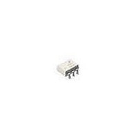
H11G2 Fairchild Semiconductor, H11G2 Datasheet

H11G2
Specifications of H11G2
Available stocks
Related parts for H11G2
H11G2 Summary of contents
Page 1
... CATHODE 2 3 N/C ©2007 Fairchild Semiconductor Corporation H11G1M, H11G2M, H11G3M Rev. 1.0.4 General Description The H11GXM series are photodarlington-type optically coupled optocouplers. These devices have a gallium arsenide infrared emitting diode coupled with a silicon darlington connected phototransistor which has an inte- gral base-emitter resistor to optimize elevated tempera- ture characteristics ...
Page 2
... LED Power Dissipation @ T D Derate Above 25°C DETECTOR V Collector-Emitter Voltage CEO H11G1M H11G2M H11G3M P Photodetector Power Dissipation @ T D Derate Above 25°C ©2007 Fairchild Semiconductor Corporation H11G1M, H11G2M, H11G3M Rev. 1.0.4 Parameter = 25° 25° 25° Value Units -40 to +150 °C -40 to +100 °C 260 for 10 sec ° ...
Page 3
... Turn-off Time OFF Isolation Characteristics Symbol Characteristic V Isolation Voltage ISO R Isolation Resistance ISO C Isolation Capacitance ISO *All Typical values 25°C A ©2007 Fairchild Semiconductor Corporation H11G1M, H11G2M, H11G3M Rev. 1.0 25°C unless otherwise specified.) A Test Conditions Device I = 10mA 10µ 0V 1MHz 1V 1MHz 3.0V ...
Page 4
... Max. Working Insulation Voltage IORM V Highest Allowable Over Voltage IOTM External Creepage External Clearance Insulation Thickness RIO Insulation Resistance at Ts, V ©2007 Fairchild Semiconductor Corporation H11G1M, H11G2M, H11G3M Rev. 1.0.4 Parameter , 100% Production Test PR , Type and Sample Test = 500V IO 4 Min. Typ. Max. ...
Page 5
... Fig. 3 Output Current vs. Collector - Emitter Voltage 100 Normalized to 1mA 25˚ 0.1 0. – COLLECTOR – EMITTER VOLTAGE (V) CE ©2007 Fairchild Semiconductor Corporation H11G1M, H11G2M, H11G3M Rev. 1.0.4 Fig. 2 Normalized Output Current vs. Temperature 100 10 Normalized to 1mA F 1 0.1 0.01 -60 10 1000 I = 50mA F 100 ...
Page 6
... Note: All dimensions in mm. ©2007 Fairchild Semiconductor Corporation H11G1M, H11G2M, H11G3M Rev. 1.0.4 0.4" Lead Spacing 6.10–6.60 7.62 (Typ.) 5.08 (Max.) 0.38 (Min.) 0.20–0.30 15° (Typ.) (0.86) 1.02–1.78 8.13– ...
Page 7
... TV SV SR2V Marking Information Definitions ©2007 Fairchild Semiconductor Corporation H11G1M, H11G2M, H11G3M Rev. 1.0.4 Order Entry Identifier (Example) H11G1M Standard Through Hole Device H11G1SM Surface Mount Lead Bend H11G1SR2M Surface Mount; Tape and Reel H11G1TM 0.4" Lead Spacing H11G1VM VDE 0884 H11G1TVM VDE 0884, 0.4" ...
Page 8
... C 140 120 100 ©2007 Fairchild Semiconductor Corporation H11G1M, H11G2M, H11G3M Rev. 1.0.4 12.0 0.1 2.0 0.05 0.05 4.0 0.1 10.1 0.20 183 Sec 1.822 C/Sec Ramp up rate 33 Sec 60 120 180 Time (s) 8 Ø1.5 MIN 1 ...
Page 9
... Datasheet Identification Product Status Advance Information Formative / In Design Preliminary First Production No Identification Needed Full Production Obsolete Not In Production ©2007 Fairchild Semiconductor Corporation H11G1M, H11G2M, H11G3M Rev. 1.0.4 ® PowerTrench ® PowerXS™ SM Programmable Active Droop™ ® QFET QS™ Quiet Series™ ...


