EA-QSB-010 Embedded Artists, EA-QSB-010 Datasheet
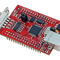
EA-QSB-010
Specifications of EA-QSB-010


Related parts for EA-QSB-010


EA-QSB-010 Summary of contents
Page 1
... For critical code size applications, the alternative 16-bit Thumb mode reduces code by more than 30 % with minimal performance penalty. Due to their tiny size and low power consumption, LPC2141/42/44/46/48 are ideal for applications where miniaturization is a key requirement, such as access control and point-of-sale ...
Page 2
... NXP Semiconductors I Low power Real-Time Clock (RTC) with independent power and 32 kHz clock input. I Multiple serial interfaces including two UARTs (16C550), two Fast I SPI and SSP with buffering and variable data length capabilities. I Vectored Interrupt Controller (VIC) with configurable priorities and vector addresses. ...
Page 3
... DECODER DIVIDER (3) USB DMA USB 2.0 FULL-SPEED DEVICE CONTROLLER (3) WITH DMA 2 I C-BUS SERIAL INTERFACES 0 AND 1 SPI AND SSP SERIAL INTERFACES UART0/UART1 REAL-TIME CLOCK WATCHDOG TIMER SYSTEM CONTROL 002aab560 D+ D UP_LED CONNECT VBUS SCL0, SCL1 SDA0, SDA1 SCK0, SCK1 MOSI0, MOSI1 ...
Page 4
NXP Semiconductors 5. Pinning information 5.1 Pinning P0.21/PWM5/CAP1.3 1 P0.22/CAP0.0/MAT0 RTCX1 4 P1.19/TRACEPKT3 RTCX2 DDA P1.18/TRACEPKT2 8 P0.25/AD0 P1.17/TRACEPKT1 12 P0.28/AD0.1/CAP0.2/MAT0 P0.29/AD0.2/CAP0.3/MAT0.3 P0.30/AD0.3/EINT3/CAP0.0 15 P1.16/TRACEPKT0 ...
Page 5
NXP Semiconductors P0.21/PWM5/CAP1.3 1 P0.22/CAP0.0/MAT0 RTCX1 P1.19/TRACEPKT3 4 RTCX2 DDA P1.18/TRACEPKT2 8 P0.25/AD0.4/AOUT P1.17/TRACEPKT1 12 P0.28/AD0.1/CAP0.2/MAT0 P0.29/AD0.2/CAP0.3/MAT0.3 P0.30/AD0.3/EINT3/CAP0.0 15 P1.16/TRACEPKT0 16 Fig 3. LPC2142 pinning ...
Page 6
NXP Semiconductors P0.21/PWM5/AD1.6/CAP1 P0.22/AD1.7/CAP0.0/MAT0.0 RTCX1 3 P1.19/TRACEPKT3 4 RTCX2 DDA P1.18/TRACEPKT2 8 9 P0.25/AD0.4/AOUT P1.17/TRACEPKT1 12 13 P0.28/AD0.1/CAP0.2/MAT0.2 P0.29/AD0.2/CAP0.3/MAT0.3 14 P0.30/AD0.3/EINT3/CAP0 P1.16/TRACEPKT0 Fig 4. LPC2144/46/48 pinning ...
Page 7
... Type Description I/O Port 0: Port 32-bit I/O port with individual direction controls for each bit. Total of 31 pins of the Port 0 can be used as a general purpose bidirectional digital I/Os while P0.31 is output only pin. The operation of port 0 pins depends upon the pin function selected via the pin connect block. ...
Page 8
... CAP1.0 — Capture input for Timer 1, channel 0. I AD1.2 — ADC 1, input 2. Available in LPC2144/46/48 only. I/O P0.11 — General purpose input/output digital pin (GPIO). I CTS1 — Clear to Send input for UART1. Available in LPC2144/46/48 only. I CAP1.1 — Capture input for Timer 1, channel 1. 2 I/O SCL1 — clock input/output ...
Page 9
NXP Semiconductors Table 3. Pin description …continued Symbol Pin [1] P0.18/CAP1.3/ 53 MISO1/MAT1.3 [1] P0.19/MAT1.2/ 54 MOSI1/CAP1.2 [2] P0.20/MAT1.3/ 55 SSEL1/EINT3 [4] P0.21/PWM5/ 1 AD1.6/CAP1.3 [4] P0.22/AD1.7/ 2 CAP0.0/MAT0.0 [1] P0.23/V 58 BUS [5] P0.25/AD0.4/ 9 AOUT [4] P0.28/AD0.1/ 13 ...
Page 10
... LOW when RESET pin is LOW or the JTAG port will be disabled. I/O Port 1: Port 32-bit bidirectional I/O port with individual direction controls for each bit. The operation of port 1 pins depends upon the pin function selected via the pin connect block. Pins 0 through 15 of port 1 are not available. I/O P1.16 — ...
Page 11
NXP Semiconductors Table 3. Pin description …continued Symbol Pin [6] P1.26/RTCK 24 [6] P1.27/TDO 64 [6] P1.28/TDI 60 [6] P1.29/TCK 56 [6] P1.30/TMS 52 [6] P1.31/TRST [8] RESET 57 [9] XTAL1 62 [9] ...
Page 12
NXP Semiconductors [ tolerant pad (no built-in pull-up resistor) providing digital I/O (with TTL levels and hysteresis and 10 ns slew rate control) and analog input function. If configured for an input function, this pad utilizes built-in glitch ...
Page 13
... ARM mode recommended to program performance critical and short code sections (such as interrupt service routines and DSP algorithms) in ARM mode. The impact on the overall code size will be minimal but the speed can be increased over Thumb mode. 6.2 On-chip flash program memory The LPC2141/42/44/46/48 incorporate a 32 kB, 64 kB, 128 kB, 256 kB and 512 kB fl ...
Page 14
NXP Semiconductors 6.3 On-chip static RAM On-chip static RAM may be used for code and/or data storage. The SRAM may be accessed as 8-bit, 16-bit, and 32-bit. The LPC2141, LPC2142/44 and LPC2146/48 provide 8 kB and 32 kB ...
Page 15
... FIQ service routine does not need to branch into the interrupt service routine but can run from the interrupt vector location. If more than one request is assigned to the FIQ class, the FIQ service routine will read a word from the VIC that identifies which FIQ source(s) is (are) requesting an interrupt. ...
Page 16
... GPIO registers. Pins may be dynamically configured as inputs or outputs. Separate registers allow setting or clearing any number of outputs simultaneously. The value of the output register may be read back, as well as the current state of the port pins. LPC2141/42/44/46/48 introduce accelerated GPIO functions over prior LPC2000 devices: • ...
Page 17
... Mbit/s data exchange with a USB host controller. It consists of a register interface, serial interface engine, endpoint buffer memory and DMA controller. The serial interface engine decodes the USB data stream and writes data to the appropriate end point buffer memory. The status of a completed USB transfer or error condition is indicated via status registers ...
Page 18
... The I C-bus is bidirectional, for inter-IC control using only two wires: a serial clock line (SCL), and a serial data line (SDA). Each device is recognized by a unique address and can operate as either a receiver-only device (e.g., an LCD driver or a transmitter with the capability to both receive and send information (such as memory)). Transmitters and/or receivers can operate in either master or slave mode, depending on whether the chip has to initiate a data transfer or is only addressed ...
Page 19
... Maximum data bit rate of one eighth of the input clock rate. 6.14 SSP serial I/O controller The LPC2141/42/44/46/48 each contain one Serial Synchronous Port controller (SSP). The SSP controller is capable of operation on a SPI, 4-wire SSI, or Microwire bus. It can interact with multiple masters and slaves on the bus. However, only a single master and a single slave can communicate on the bus during a given data transfer. The SSP supports full duplex transfers, with data frames of 4 bits to 16 bits of data fl ...
Page 20
... Selectable time period from (T T cy(PCLK) 6.17 Real-time clock The RTC is designed to provide a set of counters to measure time when normal or idle operating mode is selected. The RTC has been designed to use little power, making it suitable for battery powered systems where the CPU is not running continuously (Idle mode). ...
Page 21
... Again, the MR0 match register controls the PWM cycle rate. The other match registers control the two PWM edge positions. Additional double edge controlled PWM outputs require only two match registers each, since the repetition rate is the same for all PWM outputs. ...
Page 22
... This is important at power on, all types of reset, and whenever any of the aforementioned functions are turned off for any reason. Since the oscillator and other functions are turned off during Power-down mode, any wake-up of the processor from Power-down mode makes use of the Wake-up Timer ...
Page 23
... This feature of the LPC2141/42/44/46/48 allow an application to control whether it can be debugged or protected from observation. If after reset on-chip boot loader detects a valid checksum in flash and reads 0x8765 4321 from address 0x1FC in flash, debugging will be disabled and thus the code in flash will be protected from observation. Once debugging is disabled, it can be enabled only by performing a full chip erase using the ISP ...
Page 24
... Power-down mode reduces chip power consumption to nearly zero. Selecting an external 32 kHz clock instead of the PCLK as a clock-source for the on-chip RTC will enable the microcontroller to have the RTC active during Power-down mode. Power-down current is increased with RTC active. However significantly lower than in Idle mode ...
Page 25
... RealMonitor RealMonitor is a configurable software module, developed by ARM Inc., which enables real-time debug lightweight debug monitor that runs in the background while users debug their foreground application. It communicates with the host using the DCC, which is present in the EmbeddedICE logic. The LPC2141/42/44/46/48 contain a specific confi ...
Page 26
... This product includes circuitry specifically designed for the protection of its internal devices from the damaging effects of excessive static charge. Nonetheless suggested that conventional precautions be taken to avoid applying greater than the rated maximum. b) Parameters are valid over operating temperature range unless otherwise specified. All voltages are with respect to V otherwise noted ...
Page 27
NXP Semiconductors 8. Static characteristics Table 5. Static characteristics +85 C for commercial applications, unless otherwise specified. amb Symbol Parameter V supply voltage DD V analog supply voltage DDA V input voltage on pin i(VBAT) ...
Page 28
... I C-bus pins V HIGH-level input voltage IH V LOW-level input voltage IL V hysteresis voltage hys V LOW-level output OL voltage I input leakage current LI Oscillator pins V input voltage on pin i(XTAL1) XTAL1 LPC2141_42_44_46_48_4 Product data sheet …continued Conditions amb code while(1){} executed from flash, no active ...
Page 29
... DD [6] 3-state outputs go into 3-state mode when V [7] Please also see the errata note mentioned in errata sheet. [8] Accounts for 100 mV voltage drop in all supply lines. [9] Allowed as long as the current limit does not exceed the maximum current allowed by the device. ...
Page 30
... DDA 3.3 V SSA DDA ) is the difference between the actual step width and the ideal step width. See ) is the peak difference between the center of the steps of the actual and the ideal transfer curve after Figure 6. Figure Figure 6. Rev. 04 — 17 November 2008 LPC2141/42/44/46/48 ...
Page 31
... E O (1) Example of an actual transfer curve. (2) The ideal transfer curve. (3) Differential linearity error (E (4) Integral non-linearity (E L(adj) (5) Center of a step of the actual transfer curve. Fig 6. ADC characteristics LPC2141_42_44_46_48_4 Product data sheet (2) (5) (4) (3) 1 LSB (ideal) 1018 ...
Page 32
NXP Semiconductors ADx.y Fig 7. Suggested ADC interface - LPC2141/42/44/46/48 ADx.y pin LPC2141_42_44_46_48_4 Product data sheet LPC2141/42/44/46/ SAMPLE Rev. 04 — 17 November 2008 LPC2141/42/44/46/48 Single-chip 16-bit/32-bit microcontrollers R vsi ADx.y V ...
Page 33
NXP Semiconductors 9. Dynamic characteristics Table 7. Dynamic characteristics of USB pins (full-speed pF 1 Symbol Parameter t rise time r t fall time f t differential rise ...
Page 34
... NXP Semiconductors 9.1 Timing Fig 8. External clock timing (with an amplitude of at least V t PERIOD differential data lines Fig 9. Differential data-to-EOP transition skew and EOP width 10. Application information 10.1 Suggested USB interface solutions LPC2141/42/ 44/46/48 Fig 10. LPC2141/42/44/46/48 USB interface using the CONNECT function on pin 17 ...
Page 35
NXP Semiconductors LPC2141/42/ 44/46/48 Fig 11. LPC2141/42/44/46/48 USB interface using the UP_LED function on pin 17 LPC2141_42_44_46_48_4 Product data sheet LPC2141/42/44/46/48 Single-chip 16-bit/32-bit microcontrollers 1.5 k UP_LED VBUS ...
Page 36
... NXP Semiconductors 11. Package outline LQFP64: plastic low profile quad flat package; 64 leads; body 1 pin 1 index DIMENSIONS (mm are the original dimensions) A UNIT max. 0.20 1.45 mm 1.6 0.25 0.05 1.35 Note 1. Plastic or metal protrusions of 0.25 mm maximum per side are not included. OUTLINE VERSION ...
Page 37
NXP Semiconductors 12. Abbreviations Table 9. Acronym ADC APB BOD CPU DAC DCC DMA EOP FIFO GPIO PLL POR PWM RAM SE0 SPI SRAM SSP UART USB LPC2141_42_44_46_48_4 Product data sheet Acronym list Description Analog-to-Digital Converter Advanced Peripheral Bus Brown-Out ...
Page 38
... NXP Semiconductors 13. Revision history Table 10. Revision history Document ID Release date LPC2141_42_44_46_48_4 20081117 Modifications: LPC2141_42_44_46_48_3 20071019 LPC2141_42_44_46_48_2 20060828 LPC2141_42_44_46_48_1 20051003 LPC2141_42_44_46_48_4 Product data sheet Data sheet status Product data sheet • Replaced all occurrences of VPB with APB. • Table 3: clarified which pins do/don’t have internal pull-ups. ...
Page 39
... Qualification Product [short] data sheet Production [1] Please consult the most recently issued document before initiating or completing a design. [2] The term ‘short data sheet’ is explained in section “Definitions”. [3] The product status of device(s) described in this document may have changed since this document was published and may differ in case of multiple devices. The latest product status information is available on the Internet at URL http://www.nxp.com. 14.2 Defi ...
Page 40
... NXP Semiconductors 16. Contents 1 General description . . . . . . . . . . . . . . . . . . . . . . 1 2 Features . . . . . . . . . . . . . . . . . . . . . . . . . . . . . . . 1 2.1 Key features . . . . . . . . . . . . . . . . . . . . . . . . . . . 1 3 Ordering information . . . . . . . . . . . . . . . . . . . . . 2 3.1 Ordering options . . . . . . . . . . . . . . . . . . . . . . . . 2 4 Block diagram . . . . . . . . . . . . . . . . . . . . . . . . . . 3 5 Pinning information . . . . . . . . . . . . . . . . . . . . . . 4 5.1 Pinning . . . . . . . . . . . . . . . . . . . . . . . . . . . . . . . 4 5.2 Pin description . . . . . . . . . . . . . . . . . . . . . . . . . 7 6 Functional description . . . . . . . . . . . . . . . . . . 13 6.1 Architectural overview 6.2 On-chip flash program memory . . . . . . . . . . . 13 6.3 On-chip static RAM ...