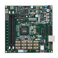
LFE3-95E-PCIE-DKN Lattice, LFE3-95E-PCIE-DKN Datasheet - Page 11

LFE3-95E-PCIE-DKN
Manufacturer Part Number
LFE3-95E-PCIE-DKN
Description
MCU, MPU & DSP Development Tools LatticeECP3 PCI Express Dev Kit
Manufacturer
Lattice
Datasheet
1.LFE3-150EA-7FN672CTW.pdf
(130 pages)
Specifications of LFE3-95E-PCIE-DKN
Processor To Be Evaluated
LFE3-95EA-x
Processor Series
LatticeECP3
Interface Type
SPI
Operating Supply Voltage
1.2 V to 3.3 V
Lead Free Status / RoHS Status
Lead free / RoHS Compliant
- Current page: 11 of 130
- Download datasheet (3Mb)
Lattice Semiconductor
chain in order to better match the reference and feedback signals. This digital code from the ALU is also transmit-
ted via the Digital Control bus (DCNTL) bus to its associated Slave Delay lines (two per DLL). The ALUHOLD input
allows the user to suspend the ALU output at its current value. The UDDCNTL signal allows the user to latch the
current value on the DCNTL bus.
The DLL has two clock outputs, CLKOP and CLKOS. These outputs can individually select one of the outputs from
the tapped delay line. The CLKOS has optional fine delay shift and divider blocks to allow this output to be further
modified, if required. The fine delay shift block allows the CLKOS output to phase shifted a further 45, 22.5 or 11.25
degrees relative to its normal position. Both the CLKOS and CLKOP outputs are available with optional duty cycle
correction. Divide by two and divide by four frequencies are available at CLKOS. The LOCK output signal is
asserted when the DLL is locked. Figure 2-5 shows the DLL block diagram and Table 2-5 provides a description of
the DLL inputs and outputs.
The user can configure the DLL for many common functions such as time reference delay mode and clock injection
removal mode. Lattice provides primitives in its design tools for these functions.
Figure 2-5. Delay Locked Loop Diagram (DLL)
GRAYI[5:0]
(CLKOP) or from a user
internal), from clock net
UDDCNTL
ALUHOLD
from CLKOP (DLL
clock (pin or logic)
or external pin)
(from routing
CLKFB
RSTN
CLKI
INCI
* This signal is not user accessible. This can only be used to feed the slave delay line.
÷4
÷2
Reference
Feedback
Detector
Phase
Arithmetic
Logic Unit
2-8
Delay Chain
Delay0
Delay1
Delay2
Delay3
Delay4
Detect
Lock
LatticeECP3 Family Data Sheet
Output
Muxes
Control
Output
Digital
Cycle
Cycle
Duty
Duty
50%
50%
÷4
÷2
6
Architecture
CLKOP
CLKOS
LOCK
DCNTL[5:0]*
DIFF
INCO
GRAYO[5:0]
Related parts for LFE3-95E-PCIE-DKN
Image
Part Number
Description
Manufacturer
Datasheet
Request
R

Part Number:
Description:
FPGA - Field Programmable Gate Array 92K LUTs, 490 I/O 8 Speed
Manufacturer:
Lattice

Part Number:
Description:
FPGA - Field Programmable Gate Array 92K LUTs, 380 I/O 7 Speed
Manufacturer:
Lattice

Part Number:
Description:
FPGA - Field Programmable Gate Array 92K LUTs, 295 I/O 7 Speed
Manufacturer:
Lattice

Part Number:
Description:
FPGA - Field Programmable Gate Array 92K LUTs, 380 I/O 6 Speed
Manufacturer:
Lattice

Part Number:
Description:
FPGA - Field Programmable Gate Array 92K LUTs, 490 I/O 6 Speed
Manufacturer:
Lattice

Part Number:
Description:
FPGA - Field Programmable Gate Array 92K LUTs, 295 I/O 8 Speed
Manufacturer:
Lattice

Part Number:
Description:
FPGA - Field Programmable Gate Array 92K LUTs, 490 I/O 8 Speed
Manufacturer:
Lattice

Part Number:
Description:
FPGA - Field Programmable Gate Array 92K LUTs, 380 I/O 8 Speed
Manufacturer:
Lattice

Part Number:
Description:
FPGA - Field Programmable Gate Array 92K LUTs, 490 I/O 6 Speed
Manufacturer:
Lattice

Part Number:
Description:
FPGA - Field Programmable Gate Array 92K LUTs, 295 I/O 6 Speed
Manufacturer:
Lattice

Part Number:
Description:
FPGA - Field Programmable Gate Array 92K LUTs, 490 I/O 7 Speed
Manufacturer:
Lattice

Part Number:
Description:
FPGA - Field Programmable Gate Array 92K LUTs, 295 I/O 8 Speed
Manufacturer:
Lattice

Part Number:
Description:
FPGA - Field Programmable Gate Array 92K LUTs, 490 I/O 7 Speed
Manufacturer:
Lattice

Part Number:
Description:
FPGA - Field Programmable Gate Array 92K LUTs, 380 I/O 6 Speed
Manufacturer:
Lattice

Part Number:
Description:
FPGA - Field Programmable Gate Array 92K LUTs, 295 I/O 7 Speed
Manufacturer:
Lattice


