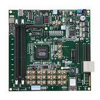
LFE3-95E-PCIE-DKN Lattice, LFE3-95E-PCIE-DKN Datasheet - Page 115

LFE3-95E-PCIE-DKN
Manufacturer Part Number
LFE3-95E-PCIE-DKN
Description
MCU, MPU & DSP Development Tools LatticeECP3 PCI Express Dev Kit
Manufacturer
Lattice
Datasheet
1.LFE3-150EA-7FN672CTW.pdf
(130 pages)
Specifications of LFE3-95E-PCIE-DKN
Processor To Be Evaluated
LFE3-95EA-x
Processor Series
LatticeECP3
Interface Type
SPI
Operating Supply Voltage
1.2 V to 3.3 V
Lead Free Status / RoHS Status
Lead free / RoHS Compliant
- Current page: 115 of 130
- Download datasheet (3Mb)
Lattice Semiconductor
Pin Information Summary (Cont.)
Emulated Differential I/O per
Bank
Highspeed Differential I/O per
Bank
Total Single Ended/ Total
Differential I/O per Bank
DDR Groups Bonded per
Bank
SERDES Quads
1. These pins must remain floating on the board.
Pin Information Summary
Pin Type
Bank 0
Bank 1
Bank 2
Bank 3
Bank 6
Bank 7
Bank 8
Bank 0
Bank 1
Bank 2
Bank 3
Bank 6
Bank 7
Bank 8
Bank 0
Bank 1
Bank 2
Bank 3
Bank 6
Bank 7
Bank 8
Bank 0
Bank 1
Bank 2
Bank 3
Bank 6
Bank 7
Configuration Bank 8
256 ftBGA
26/13
20/10
23/11
24/12
14/7
18/9
8/4
13
12
7
2
4
5
6
0
0
2
5
5
5
0
2
1
0
1
1
1
0
1
4-6
ECP3-17EA
484 fpBGA
36/18
24/12
44/22
44/22
36/18
24/12
14/7
18
12
13
13
10
12
4
0
0
3
9
9
8
0
3
2
1
3
3
2
0
1
LatticeECP3 Family Data Sheet
256 ftBGA
26/13
20/10
23/11
24/12
14/7
18/9
8/4
13
12
7
1
5
6
6
0
0
3
4
4
5
0
2
1
0
1
1
1
0
1
ECP3-35EA
484 fpBGA
Pinout Information
42/21
36/18
28/14
58/29
67/33
40/20
24/12
21
18
20
22
11
12
11
8
0
0
6
9
9
0
3
3
2
3
4
3
0
1
672 fpBGA
48/24
36/18
28/14
63/31
65/32
46/23
24/12
24
18
19
20
13
12
12
12
10
8
0
0
6
0
4
3
2
4
4
3
0
1
Related parts for LFE3-95E-PCIE-DKN
Image
Part Number
Description
Manufacturer
Datasheet
Request
R

Part Number:
Description:
FPGA - Field Programmable Gate Array 92K LUTs, 490 I/O 8 Speed
Manufacturer:
Lattice

Part Number:
Description:
FPGA - Field Programmable Gate Array 92K LUTs, 380 I/O 7 Speed
Manufacturer:
Lattice

Part Number:
Description:
FPGA - Field Programmable Gate Array 92K LUTs, 295 I/O 7 Speed
Manufacturer:
Lattice

Part Number:
Description:
FPGA - Field Programmable Gate Array 92K LUTs, 380 I/O 6 Speed
Manufacturer:
Lattice

Part Number:
Description:
FPGA - Field Programmable Gate Array 92K LUTs, 490 I/O 6 Speed
Manufacturer:
Lattice

Part Number:
Description:
FPGA - Field Programmable Gate Array 92K LUTs, 295 I/O 8 Speed
Manufacturer:
Lattice

Part Number:
Description:
FPGA - Field Programmable Gate Array 92K LUTs, 490 I/O 8 Speed
Manufacturer:
Lattice

Part Number:
Description:
FPGA - Field Programmable Gate Array 92K LUTs, 380 I/O 8 Speed
Manufacturer:
Lattice

Part Number:
Description:
FPGA - Field Programmable Gate Array 92K LUTs, 490 I/O 6 Speed
Manufacturer:
Lattice

Part Number:
Description:
FPGA - Field Programmable Gate Array 92K LUTs, 295 I/O 6 Speed
Manufacturer:
Lattice

Part Number:
Description:
FPGA - Field Programmable Gate Array 92K LUTs, 490 I/O 7 Speed
Manufacturer:
Lattice

Part Number:
Description:
FPGA - Field Programmable Gate Array 92K LUTs, 295 I/O 8 Speed
Manufacturer:
Lattice

Part Number:
Description:
FPGA - Field Programmable Gate Array 92K LUTs, 490 I/O 7 Speed
Manufacturer:
Lattice

Part Number:
Description:
FPGA - Field Programmable Gate Array 92K LUTs, 380 I/O 6 Speed
Manufacturer:
Lattice

Part Number:
Description:
FPGA - Field Programmable Gate Array 92K LUTs, 295 I/O 7 Speed
Manufacturer:
Lattice


