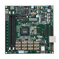
LFE3-95E-PCIE-DKN Lattice, LFE3-95E-PCIE-DKN Datasheet - Page 2

LFE3-95E-PCIE-DKN
Manufacturer Part Number
LFE3-95E-PCIE-DKN
Description
MCU, MPU & DSP Development Tools LatticeECP3 PCI Express Dev Kit
Manufacturer
Lattice
Datasheet
1.LFE3-150EA-7FN672CTW.pdf
(130 pages)
Specifications of LFE3-95E-PCIE-DKN
Processor To Be Evaluated
LFE3-95EA-x
Processor Series
LatticeECP3
Interface Type
SPI
Operating Supply Voltage
1.2 V to 3.3 V
Lead Free Status / RoHS Status
Lead free / RoHS Compliant
November 2009
Features
Higher Logic Density for Increased System
Embedded SERDES
sysDSP™
Flexible Memory Resources
sysCLOCK Analog PLLs and DLLs
Pre-Engineered Source Synchronous I/O
Table 1-1. LatticeECP3™ Family Selection Guide
© 2009 Lattice Semiconductor Corp. All Lattice trademarks, registered trademarks, patents, and disclaimers are as listed at www.latticesemi.com/legal. All other brand
or product names are trademarks or registered trademarks of their respective holders. The specifications and information herein are subject to change without notice.
www.latticesemi.com
LUTs (K)
sysMEM Blocks (18Kbits)
Embedded Memory (Kbits)
Distributed RAM Bits (Kbits)
18X18 Multipliers
SERDES (Quad)
PLLs/DLLs
Packages and SERDES Channels/ I/O Combinations
256 ftBGA (17x17 mm)
484 fpBGA (23x23 mm)
672 fpBGA (27x27 mm)
1156 fpBGA (35x35 mm)
Integration
• 17K to 149K LUTs
• 133 to 586 I/Os
• 150 Mbps to 3.2 Gbps for Generic 8b10b, 10-bit
• Data Rates 230 Mbps to 3.2 Gbps per channel
• Up to 16 channels per device: PCI Express,
• Fully cascadable slice architecture
• 12 to 160 slices for high performance multiply
• Powerful 54-bit ALU operations
• Time Division Multiplexing MAC Sharing
• Rounding and truncation
• Each slice supports
• Up to 6.85Mbits sysMEM™ Embedded Block
• 36K to 303K bits distributed RAM
• Two DLLs and up to ten PLLs per device
• DDR registers in I/O cells
SERDES, and 8-bit SERDES modes
for all other protocols
SONET/SDH, Ethernet (1GbE, SGMII, XAUI),
CPRI, SMPTE 3G and Serial RapidIO
and accumulate
RAM (EBR)
– Half 36x36, two 18x18 or four 9x9 multipliers
– Advanced 18x36 MAC and 18x18 Multiply-
Multiply-Accumulate (MMAC) operations
Device
ECP3-17
4 / 133
4 / 222
2 / 2
700
17
36
24
38
1
LatticeECP3 Family Data Sheet
ECP3-35
4 / 133
4 / 295
4 / 310
1327
4 / 2
1-1
33
68
64
72
1
Programmable sysI/O™ Buffer Supports
Flexible Device Configuration
System Level Support
Wide Range of Interfaces
• Dedicated read/write levelling functionality
• Dedicated gearing logic
• Source synchronous standards support
• Dedicated DDR/DDR2/DDR3 memory with DQS
• Optional Inter-Symbol Interference (ISI)
• On-chip termination
• Optional equalization filter on inputs
• LVTTL and LVCMOS 33/25/18/15/12
• SSTL 33/25/18/15 I, II
• HSTL15 I and HSTL18 I, II
• PCI and Differential HSTL, SSTL
• LVDS, Bus-LVDS, LVPECL, RSDS, MLVDS
• Dedicated bank for configuration I/Os
• SPI boot flash interface
• Dual-boot images supported
• Slave SPI
• TransFR™ I/O for simple field updates
• Soft Error Detect embedded macro
• IEEE 1149.1 and IEEE 1532 compliant
• Reveal Logic Analyzer
• ORCAstra FPGA configuration utility
• On-chip oscillator for initialization & general use
• 1.2V core power supply
support
correction on outputs
– ADC/DAC, 7:1 LVDS, XGMII
– High Speed ADC/DAC devices
ECP3-70
12 / 490
4 / 295
8 / 380
10 / 2
4420
145
128
240
67
3
Preliminary Data Sheet DS1021
ECP3-95
12 / 490
4 / 295
8 / 380
10 / 2
4420
Introduction
188
128
240
92
3
DS1021
Introduction_01.3
ECP3-150
16 / 586
8 / 380
10 / 2
6850
149
372
303
320
4


