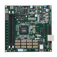
LFE3-95E-PCIE-DKN Lattice, LFE3-95E-PCIE-DKN Datasheet - Page 29

LFE3-95E-PCIE-DKN
Manufacturer Part Number
LFE3-95E-PCIE-DKN
Description
MCU, MPU & DSP Development Tools LatticeECP3 PCI Express Dev Kit
Manufacturer
Lattice
Datasheet
1.LFE3-150EA-7FN672CTW.pdf
(130 pages)
Specifications of LFE3-95E-PCIE-DKN
Processor To Be Evaluated
LFE3-95EA-x
Processor Series
LatticeECP3
Interface Type
SPI
Operating Supply Voltage
1.2 V to 3.3 V
Lead Free Status / RoHS Status
Lead free / RoHS Compliant
- Current page: 29 of 130
- Download datasheet (3Mb)
Lattice Semiconductor
MMAC DSP Element
The LatticeECP3 supports a MAC with two multipliers. This is called Multiply Multiply Accumulate or MMAC. In this
case, the two operands, AA and AB, are multiplied and the result is added with the previous accumulated value and
with the result of the multiplier operation of operands BA and BB. This accumulated value is available at the output.
The user can enable the input and pipeline registers, but the output register is always enabled. The output register
is used to store the accumulated value. The ALU is configured as the accumulator in the sysDSP slice. A registered
overflow signal is also available. The overflow conditions are provided later in this document. Figure 2-28 shows the
MMAC sysDSP element.
Figure 2-28. MMAC sysDSP Element
DSP Slice
Previous
IR = Input Register
PR = Pipeline Register
OR = Output Register
FR = Flag Register
Rounding
SRIB
SRIA
C_ALU
A_ALU
CIN
0
IR
C
IR
AA
MULTA
OR
PR
AMUX
A_ALU
IR
From FPGA Core
AB
To FPGA Core
0
R = Logic (B, C)
R= A ± B ± C
2-26
OR
PR
IR
OPCODE
FR
0
=
=
B_ALU
BMUX
IR
ALU
BA
MULTB
LatticeECP3 Family Data Sheet
OR
PR
IR
BB
IR
COUT
SROB
SROA
DSP Slice
Next
Architecture
Related parts for LFE3-95E-PCIE-DKN
Image
Part Number
Description
Manufacturer
Datasheet
Request
R

Part Number:
Description:
FPGA - Field Programmable Gate Array 92K LUTs, 490 I/O 8 Speed
Manufacturer:
Lattice

Part Number:
Description:
FPGA - Field Programmable Gate Array 92K LUTs, 380 I/O 7 Speed
Manufacturer:
Lattice

Part Number:
Description:
FPGA - Field Programmable Gate Array 92K LUTs, 295 I/O 7 Speed
Manufacturer:
Lattice

Part Number:
Description:
FPGA - Field Programmable Gate Array 92K LUTs, 380 I/O 6 Speed
Manufacturer:
Lattice

Part Number:
Description:
FPGA - Field Programmable Gate Array 92K LUTs, 490 I/O 6 Speed
Manufacturer:
Lattice

Part Number:
Description:
FPGA - Field Programmable Gate Array 92K LUTs, 295 I/O 8 Speed
Manufacturer:
Lattice

Part Number:
Description:
FPGA - Field Programmable Gate Array 92K LUTs, 490 I/O 8 Speed
Manufacturer:
Lattice

Part Number:
Description:
FPGA - Field Programmable Gate Array 92K LUTs, 380 I/O 8 Speed
Manufacturer:
Lattice

Part Number:
Description:
FPGA - Field Programmable Gate Array 92K LUTs, 490 I/O 6 Speed
Manufacturer:
Lattice

Part Number:
Description:
FPGA - Field Programmable Gate Array 92K LUTs, 295 I/O 6 Speed
Manufacturer:
Lattice

Part Number:
Description:
FPGA - Field Programmable Gate Array 92K LUTs, 490 I/O 7 Speed
Manufacturer:
Lattice

Part Number:
Description:
FPGA - Field Programmable Gate Array 92K LUTs, 295 I/O 8 Speed
Manufacturer:
Lattice

Part Number:
Description:
FPGA - Field Programmable Gate Array 92K LUTs, 490 I/O 7 Speed
Manufacturer:
Lattice

Part Number:
Description:
FPGA - Field Programmable Gate Array 92K LUTs, 380 I/O 6 Speed
Manufacturer:
Lattice

Part Number:
Description:
FPGA - Field Programmable Gate Array 92K LUTs, 295 I/O 7 Speed
Manufacturer:
Lattice


