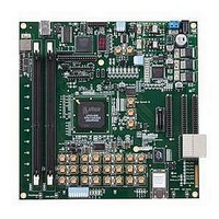
LFE3-95E-PCIE-DKN Lattice, LFE3-95E-PCIE-DKN Datasheet - Page 3

LFE3-95E-PCIE-DKN
Manufacturer Part Number
LFE3-95E-PCIE-DKN
Description
MCU, MPU & DSP Development Tools LatticeECP3 PCI Express Dev Kit
Manufacturer
Lattice
Datasheet
1.LFE3-150EA-7FN672CTW.pdf
(130 pages)
Specifications of LFE3-95E-PCIE-DKN
Processor To Be Evaluated
LFE3-95EA-x
Processor Series
LatticeECP3
Interface Type
SPI
Operating Supply Voltage
1.2 V to 3.3 V
Lead Free Status / RoHS Status
Lead free / RoHS Compliant
- Current page: 3 of 130
- Download datasheet (3Mb)
Introduction
Lattice Semiconductor
LatticeECP3 Family Data Sheet
Introduction
The LatticeECP3™ (EConomy Plus Third generation) family of FPGA devices is optimized to deliver high perfor-
mance features such as an enhanced DSP architecture, high speed SERDES and high speed source synchronous
interfaces in an economical FPGA fabric. This combination is achieved through advances in device architecture
and the use of 65nm technology making the devices suitable for high-volume, high-speed, low-cost applications.
The LatticeECP3 device family expands look-up-table (LUT) capacity to 149K logic elements and supports up to
486 user I/Os. The LatticeECP3 device family also offers up to 320 18x18 multipliers and a wide range of parallel
I/O standards.
The LatticeECP3 FPGA fabric is optimized with high performance and low cost in mind. The LatticeECP3 devices
utilize reconfigurable SRAM logic technology and provide popular building blocks such as LUT-based logic, distrib-
uted and embedded memory, Phase Locked Loops (PLLs), Delay Locked Loops (DLLs), pre-engineered source
synchronous I/O support, enhanced sysDSP slices and advanced configuration support, including encryption and
dual-boot capabilities.
The pre-engineered source synchronous logic implemented in the LatticeECP3 device family supports a broad
range of interface standards, including DDR3, XGMII and 7:1 LVDS.
The LatticeECP3 device family also features high speed SERDES with dedicated PCS functions. High jitter toler-
ance and low transmit jitter allow the SERDES plus PCS blocks to be configured to support an array of popular
data protocols including PCI Express, SMPTE, Ethernet (XAUI, GbE, and SGMII) and CPRI. Transmit Pre-empha-
sis and Receive Equalization settings make the SERDES suitable for transmission and reception over various
forms of media.
The LatticeECP3 devices also provide flexible, reliable and secure configuration options, such as dual-boot capa-
bility, bit-stream encryption, and TransFR field upgrade features.
®
The ispLEVER
design tool suite from Lattice allows large complex designs to be efficiently implemented using the
LatticeECP3 FPGA family. Synthesis library support for LatticeECP3 is available for popular logic synthesis tools.
The ispLEVER tool uses the synthesis tool output along with the constraints from its floor planning tools to place
and route the design in the LatticeECP3 device. The ispLEVER tool extracts the timing from the routing and back-
annotates it into the design for timing verification.
Lattice provides many pre-engineered IP (Intellectual Property) ispLeverCORE™ modules for the LatticeECP3
family. By using these configurable soft core IPs as standardized blocks, designers are free to concentrate on the
unique aspects of their design, increasing their productivity.
1-2
Related parts for LFE3-95E-PCIE-DKN
Image
Part Number
Description
Manufacturer
Datasheet
Request
R

Part Number:
Description:
FPGA - Field Programmable Gate Array 92K LUTs, 490 I/O 8 Speed
Manufacturer:
Lattice

Part Number:
Description:
FPGA - Field Programmable Gate Array 92K LUTs, 380 I/O 7 Speed
Manufacturer:
Lattice

Part Number:
Description:
FPGA - Field Programmable Gate Array 92K LUTs, 295 I/O 7 Speed
Manufacturer:
Lattice

Part Number:
Description:
FPGA - Field Programmable Gate Array 92K LUTs, 380 I/O 6 Speed
Manufacturer:
Lattice

Part Number:
Description:
FPGA - Field Programmable Gate Array 92K LUTs, 490 I/O 6 Speed
Manufacturer:
Lattice

Part Number:
Description:
FPGA - Field Programmable Gate Array 92K LUTs, 295 I/O 8 Speed
Manufacturer:
Lattice

Part Number:
Description:
FPGA - Field Programmable Gate Array 92K LUTs, 490 I/O 8 Speed
Manufacturer:
Lattice

Part Number:
Description:
FPGA - Field Programmable Gate Array 92K LUTs, 380 I/O 8 Speed
Manufacturer:
Lattice

Part Number:
Description:
FPGA - Field Programmable Gate Array 92K LUTs, 490 I/O 6 Speed
Manufacturer:
Lattice

Part Number:
Description:
FPGA - Field Programmable Gate Array 92K LUTs, 295 I/O 6 Speed
Manufacturer:
Lattice

Part Number:
Description:
FPGA - Field Programmable Gate Array 92K LUTs, 490 I/O 7 Speed
Manufacturer:
Lattice

Part Number:
Description:
FPGA - Field Programmable Gate Array 92K LUTs, 295 I/O 8 Speed
Manufacturer:
Lattice

Part Number:
Description:
FPGA - Field Programmable Gate Array 92K LUTs, 490 I/O 7 Speed
Manufacturer:
Lattice

Part Number:
Description:
FPGA - Field Programmable Gate Array 92K LUTs, 380 I/O 6 Speed
Manufacturer:
Lattice

Part Number:
Description:
FPGA - Field Programmable Gate Array 92K LUTs, 295 I/O 7 Speed
Manufacturer:
Lattice


