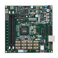
LFE3-95E-PCIE-DKN Lattice, LFE3-95E-PCIE-DKN Datasheet - Page 34

LFE3-95E-PCIE-DKN
Manufacturer Part Number
LFE3-95E-PCIE-DKN
Description
MCU, MPU & DSP Development Tools LatticeECP3 PCI Express Dev Kit
Manufacturer
Lattice
Datasheet
1.LFE3-150EA-7FN672CTW.pdf
(130 pages)
Specifications of LFE3-95E-PCIE-DKN
Processor To Be Evaluated
LFE3-95EA-x
Processor Series
LatticeECP3
Interface Type
SPI
Operating Supply Voltage
1.2 V to 3.3 V
Lead Free Status / RoHS Status
Lead free / RoHS Compliant
- Current page: 34 of 130
- Download datasheet (3Mb)
Lattice Semiconductor
Programmable I/O Cells (PIC)
Each PIC contains two PIOs connected to their respective sysI/O buffers as shown in Figure 2-32. The PIO Block
supplies the output data (DO) and the tri-state control signal (TO) to the sysI/O buffer and receives input from the
buffer. Table 2-11 provides the PIO signal list.
Figure 2-32. PIC Diagram
ECLK1, ECLK2
* Signals are available on left/right/top edges only.
** Signals are available on the left and right sides only
*** Selected PIO.
DYNDEL[7:0]
DCNTL[5:0]
ONEGA**
ONEGB**
PRMDET
DEL[3:0]
ONEGB
OPOSA
OPOSB
ECLK1
ECLK2
GSRN
READ
SCLK
SCLK
INDD
INCK
DQSI
LSR
INB
IPB
INA
IPA
CE
TS
Control
Muxes
CEOT
GSR
CLK
LSR
CEI
I/Os in a DQS-12 Group, Except DQSN (Complement of DQS) I/Os
(One per DQS Group of 12 I/Os)***
DQS Control Block
Read Control
Write Control
2-31
DDRCLKPOL*
PIOA
ECLKDQSR*
Register
Register
Tristate
Register
Output
Block
Block
Block
PIOB
DDRLAT*
DQCLK0*
DQCLK1*
(ISI)
Input
DQSW*
IOLD0
IOLT0
DI
LatticeECP3 Family Data Sheet
Buffer
sysIO
PADB
PADA
“C”
“T”
Architecture
Related parts for LFE3-95E-PCIE-DKN
Image
Part Number
Description
Manufacturer
Datasheet
Request
R

Part Number:
Description:
FPGA - Field Programmable Gate Array 92K LUTs, 490 I/O 8 Speed
Manufacturer:
Lattice

Part Number:
Description:
FPGA - Field Programmable Gate Array 92K LUTs, 380 I/O 7 Speed
Manufacturer:
Lattice

Part Number:
Description:
FPGA - Field Programmable Gate Array 92K LUTs, 295 I/O 7 Speed
Manufacturer:
Lattice

Part Number:
Description:
FPGA - Field Programmable Gate Array 92K LUTs, 380 I/O 6 Speed
Manufacturer:
Lattice

Part Number:
Description:
FPGA - Field Programmable Gate Array 92K LUTs, 490 I/O 6 Speed
Manufacturer:
Lattice

Part Number:
Description:
FPGA - Field Programmable Gate Array 92K LUTs, 295 I/O 8 Speed
Manufacturer:
Lattice

Part Number:
Description:
FPGA - Field Programmable Gate Array 92K LUTs, 490 I/O 8 Speed
Manufacturer:
Lattice

Part Number:
Description:
FPGA - Field Programmable Gate Array 92K LUTs, 380 I/O 8 Speed
Manufacturer:
Lattice

Part Number:
Description:
FPGA - Field Programmable Gate Array 92K LUTs, 490 I/O 6 Speed
Manufacturer:
Lattice

Part Number:
Description:
FPGA - Field Programmable Gate Array 92K LUTs, 295 I/O 6 Speed
Manufacturer:
Lattice

Part Number:
Description:
FPGA - Field Programmable Gate Array 92K LUTs, 490 I/O 7 Speed
Manufacturer:
Lattice

Part Number:
Description:
FPGA - Field Programmable Gate Array 92K LUTs, 295 I/O 8 Speed
Manufacturer:
Lattice

Part Number:
Description:
FPGA - Field Programmable Gate Array 92K LUTs, 490 I/O 7 Speed
Manufacturer:
Lattice

Part Number:
Description:
FPGA - Field Programmable Gate Array 92K LUTs, 380 I/O 6 Speed
Manufacturer:
Lattice

Part Number:
Description:
FPGA - Field Programmable Gate Array 92K LUTs, 295 I/O 7 Speed
Manufacturer:
Lattice


