LFE3-95E-PCIE-DKN Lattice, LFE3-95E-PCIE-DKN Datasheet - Page 35

LFE3-95E-PCIE-DKN
Manufacturer Part Number
LFE3-95E-PCIE-DKN
Description
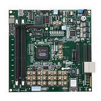
MCU, MPU & DSP Development Tools LatticeECP3 PCI Express Dev Kit
Manufacturer
Lattice
Datasheet
1.LFE3-150EA-7FN672CTW.pdf
(130 pages)
Specifications of LFE3-95E-PCIE-DKN
Processor To Be Evaluated
LFE3-95EA-x
Processor Series
LatticeECP3
Interface Type
SPI
Operating Supply Voltage
1.2 V to 3.3 V
Lead Free Status / RoHS Status
Lead free / RoHS Compliant
Lattice Semiconductor
Two adjacent PIOs can be joined to provide a differential I/O pair (labeled as “T” and “C”) as shown in Figure 2-32.
The PAD Labels “T” and “C” distinguish the two PIOs. Approximately 50% of the PIO pairs on the left and right
edges of the device can be configured as true LVDS outputs. All I/O pairs can operate as LVDS inputs.
Table 2-11. PIO Signal List
PIO
The PIO contains four blocks: an input register block, output register block, tristate register block and a control logic
block. These blocks contain registers for operating in a variety of modes along with the necessary clock and selec-
tion logic.
Input Register Block
The input register blocks for the PIOs, in the left, right and top edges, contain delay elements and registers that can
be used to condition high-speed interface signals, such as DDR memory interfaces and source synchronous inter-
faces, before they are passed to the device core. Figure 2-33 shows the input register block for the left, right and
top edges. The input register block for the bottom edge contains one element to register the input signal and no
DDR registers. The following description applies to the input register block for PIOs in the left, right and top edges
only.
INDD
IPA, INA, IPB, INB
OPOSA, ONEGA
OPOSB, ONEGB
CE
SCLK
LSR
ECLK1, ECLK2
ECLKDQSR
DDRCLKPOL
DDRLAT
DEL[3:0]
INCK
TS
DQCLK0
DQSW
DYNDEL[7:0]
DCNTL[6:0]
DATAVALID
READ
DQSI
PRMBDET
GSRN
1. Signals available on left/right/top edges only.
2. Selected PIO.
2
Name
1
1
, DQCLK1
1
1
1
1
1
,
1
To Clock Distribution
Control from routing Global Set/Reset
For DQS_Strobe
For DQS_Strobe
For DQS_Strobe
Read Control
Read Control
Read Control
Read Control
Write Control
Write Control
Write Control
Tristate Data
Output Data
Output Data
PIO Control
PIO Control
PIO Control
PIO Control
PIO Control
Input Data
Input Data
and PLL
Type
Register bypassed input. This is not the same port as INCK.
Output signals from core. An exception is the ONEGB port, used for tristate logic
at the DQS pad.
Clock enables for input and output block flip-flops.
System Clock (PCLK) for input and output/TS blocks. Connected from clock ISB.
Local Set/Reset
Edge clock sources. Entire PIO selects one of two sources using mux.
From DQS_STROBE, shifted strobe for memory interfaces only.
Ensures transfer from DQS domain to SCLK domain.
Used to guarantee INDDRX2 gearing by selectively enabling a D-Flip-Flop in dat-
apath.
Dynamic input delay control bits.
PIO treated as clock PIO, path to distribute to primary clocks and PLL.
Two clocks edges, 90 degrees out of phase, used in output gearing.
Used for output and tristate logic at DQS only.
Shifting of write clocks for specific DQS group, using 6:0 each step is approxi-
mately 25ps, 128 steps. Bit 7 is an invert (timing depends on input frequency).
There is also a static control for this 8-bit setting, enabled with a memory cell.
Original delay code from DDR DLL
IOLOGIC and valid to core.
Read signal for DDR memory interface
Unshifted DQS strobe from input pad
DQSI biased to go high when DQSI is tristate, goes to input logic block as well as
core logic.
Ports to core for input data
Tristate signal from core (SDR)
Status flag from DATAVALID logic, used to indicate when input data is captured in
2-32
Description
LatticeECP3 Family Data Sheet
Architecture


