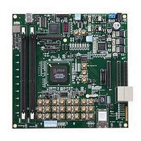
LFE3-95E-PCIE-DKN Lattice, LFE3-95E-PCIE-DKN Datasheet - Page 37

LFE3-95E-PCIE-DKN
Manufacturer Part Number
LFE3-95E-PCIE-DKN
Description
MCU, MPU & DSP Development Tools LatticeECP3 PCI Express Dev Kit
Manufacturer
Lattice
Datasheet
1.LFE3-150EA-7FN672CTW.pdf
(130 pages)
Specifications of LFE3-95E-PCIE-DKN
Processor To Be Evaluated
LFE3-95EA-x
Processor Series
LatticeECP3
Interface Type
SPI
Operating Supply Voltage
1.2 V to 3.3 V
Lead Free Status / RoHS Status
Lead free / RoHS Compliant
- Current page: 37 of 130
- Download datasheet (3Mb)
Lattice Semiconductor
Figure 2-33. ECP3-70/95 (E or EA) Input Register Block for Left, Right and Top Edges
Output Register Block
The output register block registers signals from the core of the device before they are passed to the sysI/O buffers.
The blocks on the left and right PIOs contain registers for SDR and full DDR operation. The topside PIO block is the
same as the left and right sides except it does not support ODDRX2 gearing of output logic. ODDRX2 gearing is
used in DDR3 memory interfaces.The PIO blocks on the bottom contain the SDR registers and generic DDR inter-
face without gearing.
Figure 2-34 shows the Output Register Block for PIOs on the left and right edges.
In SDR mode, OPOSA feeds one of the flip-flops that then feeds the output. The flip-flop can be configured as a
Dtype or latch. In DDR mode, two of the inputs are fed into registers on the positive edge of the clock. At the next
clock cycle, one of the registered outputs is also latched.
A multiplexer running off the same clock is used to switch the mux between the 11 and 01 inputs that will then feed
the output.
A gearbox function can be implemented in the output register block that takes four data streams: OPOSA, ONEGA,
OPOSB and ONEGB. All four data inputs are registered on the positive edge of the system clock and two of them
are also latched. The data is then output at a high rate using a multiplexer that runs off the DQCLK0 and DQCLK1
clocks. DQCLK0 and DQCLK1 are used in this case to transfer data from the system clock to the edge clock
domain. These signals are generated in the DQS Write Control Logic block. See Figure 2-37 for an overview of the
DQS write control logic.
Please see TN1180,
Further discussion on using the DQS strobe in this module is discussed in the DDR Memory section of this data
sheet.
ECLKDQSR
ECLK2
DDRCLKPOL
ECLK1
ECLK2
SCLK
DI
(From sysIO
Buffer)
DEL[3:0]
* Only on the left and right sides.
** Selected PIO.
Note: Simplified diagram does not show CE/SET/REST details.
1
0
LatticeECP3 High-Speed I/O Interface
INCLK**
INDD
To DQSI**
Dynamic Delay
Fixed Delay
0
1
A
DDR Registers
D Q
D Q
L
D Q
L
B
D Q
2-34
1 0
for more information on this topic.
CLKP
C
D
Synch Registers
D Q
D Q
F
E
D Q
D Q
L
L
LatticeECP3 Family Data Sheet
DDRLAT
H
G
D Q
D Q
Gearing Registers*
Clock Transfer &
X0
01
11
X0
01
11
D Q
D Q
L
L
K
Config bit
J
I
L
D Q
D Q
D Q
D Q
CE
Architecture
R
INB
IPB
INA
IPA
Related parts for LFE3-95E-PCIE-DKN
Image
Part Number
Description
Manufacturer
Datasheet
Request
R

Part Number:
Description:
FPGA - Field Programmable Gate Array 92K LUTs, 490 I/O 8 Speed
Manufacturer:
Lattice

Part Number:
Description:
FPGA - Field Programmable Gate Array 92K LUTs, 380 I/O 7 Speed
Manufacturer:
Lattice

Part Number:
Description:
FPGA - Field Programmable Gate Array 92K LUTs, 295 I/O 7 Speed
Manufacturer:
Lattice

Part Number:
Description:
FPGA - Field Programmable Gate Array 92K LUTs, 380 I/O 6 Speed
Manufacturer:
Lattice

Part Number:
Description:
FPGA - Field Programmable Gate Array 92K LUTs, 490 I/O 6 Speed
Manufacturer:
Lattice

Part Number:
Description:
FPGA - Field Programmable Gate Array 92K LUTs, 295 I/O 8 Speed
Manufacturer:
Lattice

Part Number:
Description:
FPGA - Field Programmable Gate Array 92K LUTs, 490 I/O 8 Speed
Manufacturer:
Lattice

Part Number:
Description:
FPGA - Field Programmable Gate Array 92K LUTs, 380 I/O 8 Speed
Manufacturer:
Lattice

Part Number:
Description:
FPGA - Field Programmable Gate Array 92K LUTs, 490 I/O 6 Speed
Manufacturer:
Lattice

Part Number:
Description:
FPGA - Field Programmable Gate Array 92K LUTs, 295 I/O 6 Speed
Manufacturer:
Lattice

Part Number:
Description:
FPGA - Field Programmable Gate Array 92K LUTs, 490 I/O 7 Speed
Manufacturer:
Lattice

Part Number:
Description:
FPGA - Field Programmable Gate Array 92K LUTs, 295 I/O 8 Speed
Manufacturer:
Lattice

Part Number:
Description:
FPGA - Field Programmable Gate Array 92K LUTs, 490 I/O 7 Speed
Manufacturer:
Lattice

Part Number:
Description:
FPGA - Field Programmable Gate Array 92K LUTs, 380 I/O 6 Speed
Manufacturer:
Lattice

Part Number:
Description:
FPGA - Field Programmable Gate Array 92K LUTs, 295 I/O 7 Speed
Manufacturer:
Lattice


