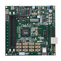
LFE3-95E-PCIE-DKN Lattice, LFE3-95E-PCIE-DKN Datasheet - Page 39

LFE3-95E-PCIE-DKN
Manufacturer Part Number
LFE3-95E-PCIE-DKN
Description
MCU, MPU & DSP Development Tools LatticeECP3 PCI Express Dev Kit
Manufacturer
Lattice
Datasheet
1.LFE3-150EA-7FN672CTW.pdf
(130 pages)
Specifications of LFE3-95E-PCIE-DKN
Processor To Be Evaluated
LFE3-95EA-x
Processor Series
LatticeECP3
Interface Type
SPI
Operating Supply Voltage
1.2 V to 3.3 V
Lead Free Status / RoHS Status
Lead free / RoHS Compliant
- Current page: 39 of 130
- Download datasheet (3Mb)
Lattice Semiconductor
Control Logic Block
The control logic block allows the selection and modification of control signals for use in the PIO block.
DDR Memory Support
Certain PICs have additional circuitry to allow the implementation of high-speed source synchronous and DDR1,
DDR2 and DDR3 memory interfaces. The support varies by the edge of the device as detailed below.
Left and Right Edges
The left and right sides of the PIC have fully functional elements supporting DDR1, DDR2, and DDR3 memory
interfaces. One of every 12 PIOs supports the dedicated DQS pins with the DQS control logic block. Figure 2-35
shows the DQS bus spanning 11 I/O pins. Two of every 12 PIOs support the dedicated DQS and DQS# pins with
the DQS control logic block.
Bottom Edge
PICs on the bottom edge of the device do not support DDR memory and Generic DDR interfaces.
Top Edge
PICs on the top side are similar to the PIO elements on the left and right sides but do not support gearing on the
output registers. Hence, the modes to support output/tristate DDR3 memory are removed on the top side.
The exact DQS pins are shown in a dual function in the Logic Signal Connections table in this data sheet. Addi-
tional detail is provided in the Signal Descriptions table. The DQS signal from the bus is used to strobe the DDR
data from the memory into input register blocks. Interfaces on the left, right and top edges are designed for DDR
memories that support 10 bits of data.
Figure 2-35. DQS Grouping on the Left, Right and Top Edges
DLL Calibrated DQS Delay Block
Source synchronous interfaces generally require the input clock to be adjusted in order to correctly capture data at
the input register. For most interfaces, a PLL is used for this adjustment. However, in DDR memories the clock
DQS
PIO A
PIO B
PIO A
PIO B
PIO A
PIO B
PIO A
PIO B
PIO A
PIO B
PIO A
PIO B
2-36
Buffer
sysIO
Delay
LatticeECP3 Family Data Sheet
PADA "T"
PADA "T"
PADA "T"
PADA "T"
PADA "T"
PADB "C"
PADB "C"
PADB "C"
PADB "C"
PADB "C"
DQS Pin
Assigned
PADA "T"
PADB "C"
LVDS Pair
LVDS Pair
LVDS Pair
LVDS Pair
LVDS Pair
LVDS Pair
Architecture
Related parts for LFE3-95E-PCIE-DKN
Image
Part Number
Description
Manufacturer
Datasheet
Request
R

Part Number:
Description:
FPGA - Field Programmable Gate Array 92K LUTs, 490 I/O 8 Speed
Manufacturer:
Lattice

Part Number:
Description:
FPGA - Field Programmable Gate Array 92K LUTs, 380 I/O 7 Speed
Manufacturer:
Lattice

Part Number:
Description:
FPGA - Field Programmable Gate Array 92K LUTs, 295 I/O 7 Speed
Manufacturer:
Lattice

Part Number:
Description:
FPGA - Field Programmable Gate Array 92K LUTs, 380 I/O 6 Speed
Manufacturer:
Lattice

Part Number:
Description:
FPGA - Field Programmable Gate Array 92K LUTs, 490 I/O 6 Speed
Manufacturer:
Lattice

Part Number:
Description:
FPGA - Field Programmable Gate Array 92K LUTs, 295 I/O 8 Speed
Manufacturer:
Lattice

Part Number:
Description:
FPGA - Field Programmable Gate Array 92K LUTs, 490 I/O 8 Speed
Manufacturer:
Lattice

Part Number:
Description:
FPGA - Field Programmable Gate Array 92K LUTs, 380 I/O 8 Speed
Manufacturer:
Lattice

Part Number:
Description:
FPGA - Field Programmable Gate Array 92K LUTs, 490 I/O 6 Speed
Manufacturer:
Lattice

Part Number:
Description:
FPGA - Field Programmable Gate Array 92K LUTs, 295 I/O 6 Speed
Manufacturer:
Lattice

Part Number:
Description:
FPGA - Field Programmable Gate Array 92K LUTs, 490 I/O 7 Speed
Manufacturer:
Lattice

Part Number:
Description:
FPGA - Field Programmable Gate Array 92K LUTs, 295 I/O 8 Speed
Manufacturer:
Lattice

Part Number:
Description:
FPGA - Field Programmable Gate Array 92K LUTs, 490 I/O 7 Speed
Manufacturer:
Lattice

Part Number:
Description:
FPGA - Field Programmable Gate Array 92K LUTs, 380 I/O 6 Speed
Manufacturer:
Lattice

Part Number:
Description:
FPGA - Field Programmable Gate Array 92K LUTs, 295 I/O 7 Speed
Manufacturer:
Lattice


