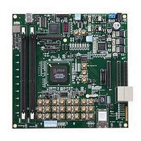
LFE3-95E-PCIE-DKN Lattice, LFE3-95E-PCIE-DKN Datasheet - Page 42

LFE3-95E-PCIE-DKN
Manufacturer Part Number
LFE3-95E-PCIE-DKN
Description
MCU, MPU & DSP Development Tools LatticeECP3 PCI Express Dev Kit
Manufacturer
Lattice
Datasheet
1.LFE3-150EA-7FN672CTW.pdf
(130 pages)
Specifications of LFE3-95E-PCIE-DKN
Processor To Be Evaluated
LFE3-95EA-x
Processor Series
LatticeECP3
Interface Type
SPI
Operating Supply Voltage
1.2 V to 3.3 V
Lead Free Status / RoHS Status
Lead free / RoHS Compliant
- Current page: 42 of 130
- Download datasheet (3Mb)
Lattice Semiconductor
Figure 2-37. DQS Local Bus
Polarity Control Logic
In a typical DDR Memory interface design, the phase relationship between the incoming delayed DQS strobe and
the internal system clock (during the READ cycle) is unknown. The LatticeECP3 family contains dedicated circuits
to transfer data between these domains. A clock polarity selector is used to prevent set-up and hold violations at
the domain transfer between DQS (delayed) and the system clock. This changes the edge on which the data is reg-
istered in the synchronizing registers in the input register block. This requires evaluation at the start of each READ
cycle for the correct clock polarity.
Prior to the READ operation in DDR memories, DQS is in tristate (pulled by termination). The DDR memory device
drives DQS low at the start of the preamble state. A dedicated circuit detects the first DQS rising edge after the pre-
amble state. This signal is used to control the polarity of the clock to the synchronizing registers.
DDR3 Memory Support
LatticeECP3 supports the read and write leveling required for DDR3 memory interfaces.
Read leveling is supported by the use of the DDRCLKPOL and the DDRLAT signals generated in the DQS Read
Control logic block. These signals dynamically control the capture of the data with respect to the DQS at the input
register block.
Data Output Register Block
DQS Output Register Block
Data Input Register Block
DQS Write Control Logic
DQS Read Control Logic
DQS Delay Block
DDR DLL
2-39
LatticeECP3 Family Data Sheet
DDR Data
Pad
DQS
Pad
Architecture
Related parts for LFE3-95E-PCIE-DKN
Image
Part Number
Description
Manufacturer
Datasheet
Request
R

Part Number:
Description:
FPGA - Field Programmable Gate Array 92K LUTs, 490 I/O 8 Speed
Manufacturer:
Lattice

Part Number:
Description:
FPGA - Field Programmable Gate Array 92K LUTs, 380 I/O 7 Speed
Manufacturer:
Lattice

Part Number:
Description:
FPGA - Field Programmable Gate Array 92K LUTs, 295 I/O 7 Speed
Manufacturer:
Lattice

Part Number:
Description:
FPGA - Field Programmable Gate Array 92K LUTs, 380 I/O 6 Speed
Manufacturer:
Lattice

Part Number:
Description:
FPGA - Field Programmable Gate Array 92K LUTs, 490 I/O 6 Speed
Manufacturer:
Lattice

Part Number:
Description:
FPGA - Field Programmable Gate Array 92K LUTs, 295 I/O 8 Speed
Manufacturer:
Lattice

Part Number:
Description:
FPGA - Field Programmable Gate Array 92K LUTs, 490 I/O 8 Speed
Manufacturer:
Lattice

Part Number:
Description:
FPGA - Field Programmable Gate Array 92K LUTs, 380 I/O 8 Speed
Manufacturer:
Lattice

Part Number:
Description:
FPGA - Field Programmable Gate Array 92K LUTs, 490 I/O 6 Speed
Manufacturer:
Lattice

Part Number:
Description:
FPGA - Field Programmable Gate Array 92K LUTs, 295 I/O 6 Speed
Manufacturer:
Lattice

Part Number:
Description:
FPGA - Field Programmable Gate Array 92K LUTs, 490 I/O 7 Speed
Manufacturer:
Lattice

Part Number:
Description:
FPGA - Field Programmable Gate Array 92K LUTs, 295 I/O 8 Speed
Manufacturer:
Lattice

Part Number:
Description:
FPGA - Field Programmable Gate Array 92K LUTs, 490 I/O 7 Speed
Manufacturer:
Lattice

Part Number:
Description:
FPGA - Field Programmable Gate Array 92K LUTs, 380 I/O 6 Speed
Manufacturer:
Lattice

Part Number:
Description:
FPGA - Field Programmable Gate Array 92K LUTs, 295 I/O 7 Speed
Manufacturer:
Lattice


