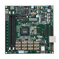
LFE3-95E-PCIE-DKN Lattice, LFE3-95E-PCIE-DKN Datasheet - Page 49

LFE3-95E-PCIE-DKN
Manufacturer Part Number
LFE3-95E-PCIE-DKN
Description
MCU, MPU & DSP Development Tools LatticeECP3 PCI Express Dev Kit
Manufacturer
Lattice
Datasheet
1.LFE3-150EA-7FN672CTW.pdf
(130 pages)
Specifications of LFE3-95E-PCIE-DKN
Processor To Be Evaluated
LFE3-95EA-x
Processor Series
LatticeECP3
Interface Type
SPI
Operating Supply Voltage
1.2 V to 3.3 V
Lead Free Status / RoHS Status
Lead free / RoHS Compliant
- Current page: 49 of 130
- Download datasheet (3Mb)
Lattice Semiconductor
Table 2-14. Available SERDES Quads per LatticeECP3 Devices
SERDES Block
A SERDES receiver channel may receive the serial differential data stream, equalize the signal, perform Clock and
Data Recovery (CDR) and de-serialize the data stream before passing the 8- or 10-bit data to the PCS logic. The
SERDES transmitter channel may receive the parallel 8- or 10-bit data, serialize the data and transmit the serial bit
stream through the differential drivers. Figure 2-41 shows a single-channel SERDES/PCS block. Each SERDES
channel provides a recovered clock and a SERDES transmit clock to the PCS block and to the FPGA core logic.
Each transmit channel, receiver channel, and SERDES PLL shares the same power supply (VCCA). The output
and input buffers of each channel have their own independent power supplies (VCCOB and VCCIB).
Figure 2-41. Simplified Channel Block Diagram for SERDES/PCS Block
PCS
As shown in Figure 2-41, the PCS receives the parallel digital data from the deserializer and selects the polarity,
performs word alignment, decodes (8b/10b), provides Clock Tolerance Compensation and transfers the clock
domain from the recovered clock to the FPGA clock via the Down Sample FIFO.
For the transmit channel, the PCS block receives the parallel data from the FPGA core, encodes it with 8b/10b,
selects the polarity and passes the 8/10 bit data to the transmit SERDES channel.
The PCS also provides bypass modes that allow a direct 8-bit or 10-bit interface from the SERDES to the FPGA
logic. The PCS interface to the FPGA can also be programmed to run at 1/2 speed for a 16-bit or 20-bit interface to
the FPGA logic.
SCI (SERDES Client Interface) Bus
The SERDES Client Interface (SCI) is an IP interface that allows the SERDES/PCS Quad block to be controlled by
registers rather than the configuration memory cells. It is a simple register configuration interface that allows
SERDES/PCS configuration without power cycling the device.
256 ftBGA
484 ftBGA
672 ftBGA
1156 ftBGA
HDOUTN
HDOUTP
HDINN
HDINP
Package
* 1/8 or 1/10 line rate
TX REFCLK
Receiver
Transmitter
RX_REFCLK
Equalizer
TX PLL
SERDES
Clock/Data
ECP3-17
Recovery
Serializer
8:1/10:1
—
—
1
1
Clock
Data
Deserializer
1:8/1:10
ECP3-35
—
1
1
1
Recovered Clock*
SERDES Transmit Clock*
Bypass
Polarity
Polarity
Adjust
Adjust
Bypass
2-46
Word Alignment
8b10b Decoder
ECP3-70
Bypass
—
1
2
3
Encoder
Bypass
8b10b
PCS
Bypass
LatticeECP3 Family Data Sheet
CTC
ECP3-95
—
1
2
3
Upsample
FIFO
Downsample
FIFO
Architecture
Receive Clock
Transmit Data
Transmit Clock
FPGA Core
ECP3-150
Recovered Clock
Receive Data
SERDES Transmit Clock
—
2
4
Related parts for LFE3-95E-PCIE-DKN
Image
Part Number
Description
Manufacturer
Datasheet
Request
R

Part Number:
Description:
FPGA - Field Programmable Gate Array 92K LUTs, 490 I/O 8 Speed
Manufacturer:
Lattice

Part Number:
Description:
FPGA - Field Programmable Gate Array 92K LUTs, 380 I/O 7 Speed
Manufacturer:
Lattice

Part Number:
Description:
FPGA - Field Programmable Gate Array 92K LUTs, 295 I/O 7 Speed
Manufacturer:
Lattice

Part Number:
Description:
FPGA - Field Programmable Gate Array 92K LUTs, 380 I/O 6 Speed
Manufacturer:
Lattice

Part Number:
Description:
FPGA - Field Programmable Gate Array 92K LUTs, 490 I/O 6 Speed
Manufacturer:
Lattice

Part Number:
Description:
FPGA - Field Programmable Gate Array 92K LUTs, 295 I/O 8 Speed
Manufacturer:
Lattice

Part Number:
Description:
FPGA - Field Programmable Gate Array 92K LUTs, 490 I/O 8 Speed
Manufacturer:
Lattice

Part Number:
Description:
FPGA - Field Programmable Gate Array 92K LUTs, 380 I/O 8 Speed
Manufacturer:
Lattice

Part Number:
Description:
FPGA - Field Programmable Gate Array 92K LUTs, 490 I/O 6 Speed
Manufacturer:
Lattice

Part Number:
Description:
FPGA - Field Programmable Gate Array 92K LUTs, 295 I/O 6 Speed
Manufacturer:
Lattice

Part Number:
Description:
FPGA - Field Programmable Gate Array 92K LUTs, 490 I/O 7 Speed
Manufacturer:
Lattice

Part Number:
Description:
FPGA - Field Programmable Gate Array 92K LUTs, 295 I/O 8 Speed
Manufacturer:
Lattice

Part Number:
Description:
FPGA - Field Programmable Gate Array 92K LUTs, 490 I/O 7 Speed
Manufacturer:
Lattice

Part Number:
Description:
FPGA - Field Programmable Gate Array 92K LUTs, 380 I/O 6 Speed
Manufacturer:
Lattice

Part Number:
Description:
FPGA - Field Programmable Gate Array 92K LUTs, 295 I/O 7 Speed
Manufacturer:
Lattice


