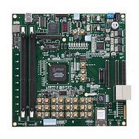
LFE3-95E-PCIE-DKN Lattice, LFE3-95E-PCIE-DKN Datasheet - Page 50

LFE3-95E-PCIE-DKN
Manufacturer Part Number
LFE3-95E-PCIE-DKN
Description
MCU, MPU & DSP Development Tools LatticeECP3 PCI Express Dev Kit
Manufacturer
Lattice
Datasheet
1.LFE3-150EA-7FN672CTW.pdf
(130 pages)
Specifications of LFE3-95E-PCIE-DKN
Processor To Be Evaluated
LFE3-95EA-x
Processor Series
LatticeECP3
Interface Type
SPI
Operating Supply Voltage
1.2 V to 3.3 V
Lead Free Status / RoHS Status
Lead free / RoHS Compliant
Lattice Semiconductor
The ispLEVER design tools from Lattice support all modes of the PCS. Most modes are dedicated to applications
associated with a specific industry standard data protocol. Other more general purpose modes allow users to
define their own operation. With ispLEVER, the user can define the mode for each quad in a design.
Popular standards such as 10Gb Ethernet, x4 PCI Express and 4x Serial RapidIO can be implemented using IP
(available through Lattice), a single quad (Four SERDES channels and PCS) and some additional logic from the
core.
The LatticeECP3 family also supports a wide range of primary and secondary protocols. Within the same quad, the
LatticeECP3 family can support mixed protocols with semi-independent clocking as long as the required clock fre-
quencies are integer x1, x2, or x11 multiples of each other. Table 2-15 lists the allowable combination of primary
and secondary protocol combinations.
Flexible Quad SERDES Architecture
The LatticeECP3 family SERDES architecture is a quad-based architecture. For most SERDES settings and stan-
dards, the whole quad (consisting of four SERDES) is treated as a unit. This helps in silicon area savings, better
utilization and overall lower cost.
However, for some specific standards, the LatticeECP3 quad architecture provides flexibility; more than one stan-
dard can be supported within the same quad.
Table 2-15 shows the standards can be mixed and matched within the same quad. In general, the SERDES stan-
dards whose nominal data rates are either the same or a defined subset of each other, can be supported within the
same quad. In Table 2-15, the Primary Protocol column refers to the standard that determines the reference clock
and PLL settings. The Secondary Protocol column shows the other standard that can be supported within the
same quad.
Furthermore, Table 2-15 also implies that more than two standards in the same quad can be supported, as long as
they conform to the data rate and reference clock requirements. For example, a quad may contain PCI Express 1.1,
SGMII, Serial RapidIO Type I and Serial RapidIO Type II, all in the same quad.
Table 2-15. LatticeECP3 Primary and Secondary Protocol Support
For further information on SERDES, please see TN1176,
IEEE 1149.1-Compliant Boundary Scan Testability
All LatticeECP3 devices have boundary scan cells that are accessed through an IEEE 1149.1 compliant Test
Access Port (TAP). This allows functional testing of the circuit board on which the device is mounted through a
serial scan path that can access all critical logic nodes. Internal registers are linked internally, allowing test data to
be shifted in and loaded directly onto test nodes, or test data to be captured and shifted out for verification. The test
PCI Express 1.1
PCI Express 1.1
PCI Express 1.1
PCI Express 1.1
Serial RapidIO Type I
Serial RapidIO Type I
Serial RapidIO Type II
Serial RapidIO Type II
Serial RapidIO Type II
CPRI-3
3G-SDI
Primary Protocol
2-47
SGMII
Gigabit Ethernet
Serial RapidIO Type I
Serial RapidIO Type II
SGMII
Gigabit Ethernet
SGMII
Gigabit Ethernet
Serial RapidIO Type I
CPRI-2 and CPRI-1
HD-SDI and SD-SDI
LatticeECP3 SERDES/PCS Usage
Secondary Protocol
LatticeECP3 Family Data Sheet
Guide.
Architecture


