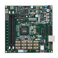
LFE3-95E-PCIE-DKN Lattice, LFE3-95E-PCIE-DKN Datasheet - Page 52

LFE3-95E-PCIE-DKN
Manufacturer Part Number
LFE3-95E-PCIE-DKN
Description
MCU, MPU & DSP Development Tools LatticeECP3 PCI Express Dev Kit
Manufacturer
Lattice
Datasheet
1.LFE3-150EA-7FN672CTW.pdf
(130 pages)
Specifications of LFE3-95E-PCIE-DKN
Processor To Be Evaluated
LFE3-95EA-x
Processor Series
LatticeECP3
Interface Type
SPI
Operating Supply Voltage
1.2 V to 3.3 V
Lead Free Status / RoHS Status
Lead free / RoHS Compliant
- Current page: 52 of 130
- Download datasheet (3Mb)
Lattice Semiconductor
can also be programmed to utilize a Soft Error Detect (SED) mode that checks for soft errors in configuration
SRAM. The SED operation can be run in the background during user mode. If a soft error occurs, during user
mode (normal operation) the device can be programmed to generate an error signal.
For further information on SED support, please see TN1184,
Guide.
External Resistor
LatticeECP3 devices require a single external, 10K ohm ±1% value between the XRES pin and ground. Device
con• guration will not be completed if this resistor is missing. There is no boundary scan register on the external
resistor pad.
On-Chip Oscillator
Every LatticeECP3 device has an internal CMOS oscillator which is used to derive a Master Clock (MCLK) for con-
figuration. The oscillator and the MCLK run continuously and are available to user logic after configuration is com-
pleted. The software default value of the MCLK is nominally 2.5MHz. Table 2-16 lists all the available MCLK
frequencies. When a different Master Clock is selected during the design process, the following sequence takes
place:
1. Device powers up with a nominal Master Clock frequency of 3.1MHz.
2. During configuration, users select a different master clock frequency.
3. The Master Clock frequency changes to the selected frequency once the clock configuration bits are received.
4. If the user does not select a master clock frequency, then the configuration bitstream defaults to the MCLK fre-
This internal CMOS oscillator is available to the user by routing it as an input clock to the clock tree. For further
information on the use of this oscillator for configuration or user mode, please see TN1169,
FIG Usage
Table 2-16. Selectable Master Clock (MCLK) Frequencies During Configuration (Nominal)
Density Shifting
The LatticeECP3 family is designed to ensure that different density devices in the same family and in the same
package have the same pinout. Furthermore, the architecture ensures a high success rate when performing design
migration from lower density devices to higher density devices. In many cases, it is also possible to shift a lower uti-
lization design targeted for a high-density device to a lower density device. However, the exact details of the final
resource utilization will impact the likelihood of success in each case. An example is that some user I/Os may
become No Connects in smaller devices in the same packge.
quency of 2.5MHz.
Guide.
1. Software default MCLK frequency. Hardware default is
MCLK (MHz)
3.1MHz.
2.5
3.1
4.3
5.4
6.9
8.1
9.2
1
MCLK (MHz)
2-49
10
13
15
20
26
30
34
LatticeECP3 Soft Error Detection (SED) Usage
MCLK (MHz)
130
41
45
51
55
60
—
LatticeECP3 Family Data Sheet
LatticeECP3 sysCON-
Architecture
Related parts for LFE3-95E-PCIE-DKN
Image
Part Number
Description
Manufacturer
Datasheet
Request
R

Part Number:
Description:
FPGA - Field Programmable Gate Array 92K LUTs, 490 I/O 8 Speed
Manufacturer:
Lattice

Part Number:
Description:
FPGA - Field Programmable Gate Array 92K LUTs, 380 I/O 7 Speed
Manufacturer:
Lattice

Part Number:
Description:
FPGA - Field Programmable Gate Array 92K LUTs, 295 I/O 7 Speed
Manufacturer:
Lattice

Part Number:
Description:
FPGA - Field Programmable Gate Array 92K LUTs, 380 I/O 6 Speed
Manufacturer:
Lattice

Part Number:
Description:
FPGA - Field Programmable Gate Array 92K LUTs, 490 I/O 6 Speed
Manufacturer:
Lattice

Part Number:
Description:
FPGA - Field Programmable Gate Array 92K LUTs, 295 I/O 8 Speed
Manufacturer:
Lattice

Part Number:
Description:
FPGA - Field Programmable Gate Array 92K LUTs, 490 I/O 8 Speed
Manufacturer:
Lattice

Part Number:
Description:
FPGA - Field Programmable Gate Array 92K LUTs, 380 I/O 8 Speed
Manufacturer:
Lattice

Part Number:
Description:
FPGA - Field Programmable Gate Array 92K LUTs, 490 I/O 6 Speed
Manufacturer:
Lattice

Part Number:
Description:
FPGA - Field Programmable Gate Array 92K LUTs, 295 I/O 6 Speed
Manufacturer:
Lattice

Part Number:
Description:
FPGA - Field Programmable Gate Array 92K LUTs, 490 I/O 7 Speed
Manufacturer:
Lattice

Part Number:
Description:
FPGA - Field Programmable Gate Array 92K LUTs, 295 I/O 8 Speed
Manufacturer:
Lattice

Part Number:
Description:
FPGA - Field Programmable Gate Array 92K LUTs, 490 I/O 7 Speed
Manufacturer:
Lattice

Part Number:
Description:
FPGA - Field Programmable Gate Array 92K LUTs, 380 I/O 6 Speed
Manufacturer:
Lattice

Part Number:
Description:
FPGA - Field Programmable Gate Array 92K LUTs, 295 I/O 7 Speed
Manufacturer:
Lattice


