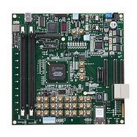
LFE3-95E-PCIE-DKN Lattice, LFE3-95E-PCIE-DKN Datasheet - Page 53

LFE3-95E-PCIE-DKN
Manufacturer Part Number
LFE3-95E-PCIE-DKN
Description
MCU, MPU & DSP Development Tools LatticeECP3 PCI Express Dev Kit
Manufacturer
Lattice
Datasheet
1.LFE3-150EA-7FN672CTW.pdf
(130 pages)
Specifications of LFE3-95E-PCIE-DKN
Processor To Be Evaluated
LFE3-95EA-x
Processor Series
LatticeECP3
Interface Type
SPI
Operating Supply Voltage
1.2 V to 3.3 V
Lead Free Status / RoHS Status
Lead free / RoHS Compliant
Absolute Maximum Ratings
1. Stress above those listed under the “Absolute Maximum Ratings” may cause permanent damage to the device. Functional operation of the
2. Compliance with the Lattice
3. All voltages referenced to GND.
4. Overshoot and undershoot of -2V to (V
March 2010
Recommended Operating Conditions
© 2010 Lattice Semiconductor Corp. All Lattice trademarks, registered trademarks, patents, and disclaimers are as listed at www.latticesemi.com/legal. All other brand
or product names are trademarks or registered trademarks of their respective holders. The specifications and information herein are subject to change without notice.
www.latticesemi.com
Supply Voltage V
Supply Voltage V
Supply Voltage V
Output Supply Voltage V
Input or I/O Tristate Voltage Applied
Storage Temperature (Ambient) . . . . . . . . . -65 to 150°C
Junction Temperature (Tj) . . . . . . . . . . . . . . . . . . +125°C
V
V
V
V
V
V
V
t
t
SERDES External Power Supply
V
V
V
1. For correct operation, all supplies except V
2. If V
3. See recommended voltages by I/O standard in subsequent table.
4. V
5. If not used, V
6. See TN1176,
JCOM
JIND
CC
CCAUX
CCPLL
CCIO
CCJ
REF1
TT
CCIB
CCOB
CCA
device at these or any other conditions above those indicated in the operational sections of this specification is not implied.
usage.
nected to the same power supply as V
5
CCAUX
2
2
CCIO
2, 3
and V
2, 4
Symbol
ramp rate must not exceed 30mV/µs during power-up when transitioning between 0V and 3.3V.
or V
REF2
CCJ
TT
LatticeECP3 SERDES/PCS Usage Guide
should be left floating.
is set to 1.2V, they must be connected to the same power supply as V
CC
CCAUX
CCJ
. . . . . . . . . . . . . . . . . . . -0.5 to 1.32V
. . . . . . . . . . . . . . . . . . -0.5 to 3.75V
Core Supply Voltage
Auxiliary Supply Voltage, Terminating Resistor Switching Power
Supply (SERDES)
PLL Supply Voltage
I/O Driver Supply Voltage
Supply Voltage for IEEE 1149.1 Test Access Port
Input Reference Voltage
Termination Voltage
Junction Temperature, Commercial Operation
Junction Temperature, Industrial Operation
Input Buffer Power Supply (1.2V)
Input Buffer Power Supply (1.5V)
Output Buffer Power Supply (1.2V)
Output Buffer Power Supply (1.5V)
Transmit, Receive, PLL and Reference Clock Buffer Power Supply
. . . . . . . . . . . . . . . . -0.5 to 3.75V
CCIO
Thermal Management
. . . . . . . . . . . -0.5 to 3.75V
6
IHMAX
CCAUX
4
. . . . . . -0.5 to 3.75V
REF
+ 2) volts is permitted for a duration of <20ns.
.
and V
1, 2, 3
DC and Switching Characteristics
document is required.
TT
LatticeECP3 Family Data Sheet
must be held in their valid operation range. This is true independent of feature
for information on board considerations for SERDES power supplies.
Parameter
3-1
1
CC.
If V
CCIO
or V
Preliminary Data Sheet DS1021
DS1021
CCJ
3.135
3.135
1.425
1.425
Min.
1.14
1.14
1.14
1.14
1.14
1.14
-40
is set to 3.3V, they must be con-
0.5
0.5
0
DC and Switching_01.7
1.3125
3.465
3.465
3.465
3.465
1.575
1.575
Max.
1.26
1.26
1.26
1.26
100
1.7
85
Units
°C
°C
V
V
V
V
V
V
V
V
V
V
V
V


