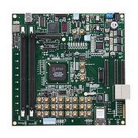
LFE3-95E-PCIE-DKN Lattice, LFE3-95E-PCIE-DKN Datasheet - Page 54

LFE3-95E-PCIE-DKN
Manufacturer Part Number
LFE3-95E-PCIE-DKN
Description
MCU, MPU & DSP Development Tools LatticeECP3 PCI Express Dev Kit
Manufacturer
Lattice
Datasheet
1.LFE3-150EA-7FN672CTW.pdf
(130 pages)
Specifications of LFE3-95E-PCIE-DKN
Processor To Be Evaluated
LFE3-95EA-x
Processor Series
LatticeECP3
Interface Type
SPI
Operating Supply Voltage
1.2 V to 3.3 V
Lead Free Status / RoHS Status
Lead free / RoHS Compliant
- Current page: 54 of 130
- Download datasheet (3Mb)
Lattice Semiconductor
Hot Socketing Specifications
Hot Socketing Requirements
ESD Performance
IDK_HS
IDK
1. V
2. Applicable to general purpose I/O pins in top I/O banks only.
3. I
4. LVCMOS and LVTTL only.
5. Applicable to general purpose I/O pins in left and right I/O banks only.
Input current per SERDES I/O pin when device is powered down and inputs
driven.
1. Assumes the device is powered down, all supplies grounded, both P and N inputs driven by CML driver with maximum allowed VCCOB
2. Each P and N input must have less than the specified maximum input current. For a 16-channel device, the total input current would be
Symbol
(1.575V), 8b10b data, internal AC coupling.
8mA*16 channels *2 input pins per channel = 256mA
DK
5
CC
is additive to I
, V
All pins
All pins except high-speed serial and XRES
High-speed serial inputs
1. The XRES pin on the TW device passes CDM testing at 250V.
2
CCAUX
Input or I/O Leakage Current
Input or I/O Leakage Current
and V
PU
CCIO
, I
PW
Parameter
should rise/fall monotonically.
Pin Group
or I
BH
.
Description
0 V
0 V
V
CCIO
1, 2
1, 3, 4
IN
IN
1
V
V
< V
Condition
IN
IH
CCIO
V
(Max.)
ESD Stress
CCIO
3-2
HBM
CDM
CDM
+ 0.5V
DC and Switching Characteristics
Min.
Min.
—
—
—
—
LatticeECP3 Family Data Sheet
1000
Min.
500
400
Typ.
Typ.
18
—
—
—
Max.
Max.
+/-1
+/-1
Units
—
8
V
V
V
Units
Units
mA
mA
mA
mA
Related parts for LFE3-95E-PCIE-DKN
Image
Part Number
Description
Manufacturer
Datasheet
Request
R

Part Number:
Description:
FPGA - Field Programmable Gate Array 92K LUTs, 490 I/O 8 Speed
Manufacturer:
Lattice

Part Number:
Description:
FPGA - Field Programmable Gate Array 92K LUTs, 380 I/O 7 Speed
Manufacturer:
Lattice

Part Number:
Description:
FPGA - Field Programmable Gate Array 92K LUTs, 295 I/O 7 Speed
Manufacturer:
Lattice

Part Number:
Description:
FPGA - Field Programmable Gate Array 92K LUTs, 380 I/O 6 Speed
Manufacturer:
Lattice

Part Number:
Description:
FPGA - Field Programmable Gate Array 92K LUTs, 490 I/O 6 Speed
Manufacturer:
Lattice

Part Number:
Description:
FPGA - Field Programmable Gate Array 92K LUTs, 295 I/O 8 Speed
Manufacturer:
Lattice

Part Number:
Description:
FPGA - Field Programmable Gate Array 92K LUTs, 490 I/O 8 Speed
Manufacturer:
Lattice

Part Number:
Description:
FPGA - Field Programmable Gate Array 92K LUTs, 380 I/O 8 Speed
Manufacturer:
Lattice

Part Number:
Description:
FPGA - Field Programmable Gate Array 92K LUTs, 490 I/O 6 Speed
Manufacturer:
Lattice

Part Number:
Description:
FPGA - Field Programmable Gate Array 92K LUTs, 295 I/O 6 Speed
Manufacturer:
Lattice

Part Number:
Description:
FPGA - Field Programmable Gate Array 92K LUTs, 490 I/O 7 Speed
Manufacturer:
Lattice

Part Number:
Description:
FPGA - Field Programmable Gate Array 92K LUTs, 295 I/O 8 Speed
Manufacturer:
Lattice

Part Number:
Description:
FPGA - Field Programmable Gate Array 92K LUTs, 490 I/O 7 Speed
Manufacturer:
Lattice

Part Number:
Description:
FPGA - Field Programmable Gate Array 92K LUTs, 380 I/O 6 Speed
Manufacturer:
Lattice

Part Number:
Description:
FPGA - Field Programmable Gate Array 92K LUTs, 295 I/O 7 Speed
Manufacturer:
Lattice


