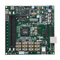
LFE3-95E-PCIE-DKN Lattice, LFE3-95E-PCIE-DKN Datasheet - Page 62

LFE3-95E-PCIE-DKN
Manufacturer Part Number
LFE3-95E-PCIE-DKN
Description
MCU, MPU & DSP Development Tools LatticeECP3 PCI Express Dev Kit
Manufacturer
Lattice
Datasheet
1.LFE3-150EA-7FN672CTW.pdf
(130 pages)
Specifications of LFE3-95E-PCIE-DKN
Processor To Be Evaluated
LFE3-95EA-x
Processor Series
LatticeECP3
Interface Type
SPI
Operating Supply Voltage
1.2 V to 3.3 V
Lead Free Status / RoHS Status
Lead free / RoHS Compliant
- Current page: 62 of 130
- Download datasheet (3Mb)
Lattice Semiconductor
BLVDS25
The LatticeECP3 devices support the BLVDS standard. This standard is emulated using complementary LVCMOS
outputs in conjunction with a parallel external resistor across the driver outputs. BLVDS is intended for use when
multi-drop and bi-directional multi-point differential signaling is required. The scheme shown in Figure 3-2 is one
possible solution for bi-directional multi-point differential signals.
Figure 3-2. BLVDS25 Multi-point Output Example
Table 3-2. BLVDS25 DC Conditions
V
Z
R
R
R
V
V
V
V
I
1. For input buffer, see LVDS table.
DC
16mA
16mA
OUT
CCIO
OH
OL
OD
CM
S
TL
TR
Parameter
2.5V
2.5V
+
-
R
R
Output Driver Supply (+/- 5%)
Driver Impedance
Driver Series Resistor (+/- 1%)
Driver Parallel Resistor (+/- 1%)
Receiver Termination (+/- 1%)
Output High Voltage
Output Low Voltage
Output Differential Voltage
Output Common Mode Voltage
DC Output Current
90 ohms
S
S
45-90
ohms
= 90 ohms
R
= 90 ohms
Heavily loaded backplane, effective Zo ~ 45 to 90 ohms differential
S
=
2.5V
Over Recommended Operating Conditions
R
1
16mA
TL
Description
90 ohms
2.5V
R
S
=
16mA
3-10
-
. . .
. . .
90 ohms
R
2.5V
S
=
16mA
Zo = 45
10.00
90.00
45.00
45.00
11.24
2.50
1.38
1.12
0.25
1.25
90 ohms
DC and Switching Characteristics
R
2.5V
S
45-90
ohms
Typical
=
LatticeECP3 Family Data Sheet
16mA
Zo = 90
90 ohms
90 ohms
10.00
90.00
90.00
90.00
10.20
R
R
2.50
1.48
1.02
0.46
1.25
R
S
S
TR
=
=
-
Units
2.5V
2.5V
mA
V
V
V
V
V
16mA
16mA
+
-
Related parts for LFE3-95E-PCIE-DKN
Image
Part Number
Description
Manufacturer
Datasheet
Request
R

Part Number:
Description:
FPGA - Field Programmable Gate Array 92K LUTs, 490 I/O 8 Speed
Manufacturer:
Lattice

Part Number:
Description:
FPGA - Field Programmable Gate Array 92K LUTs, 380 I/O 7 Speed
Manufacturer:
Lattice

Part Number:
Description:
FPGA - Field Programmable Gate Array 92K LUTs, 295 I/O 7 Speed
Manufacturer:
Lattice

Part Number:
Description:
FPGA - Field Programmable Gate Array 92K LUTs, 380 I/O 6 Speed
Manufacturer:
Lattice

Part Number:
Description:
FPGA - Field Programmable Gate Array 92K LUTs, 490 I/O 6 Speed
Manufacturer:
Lattice

Part Number:
Description:
FPGA - Field Programmable Gate Array 92K LUTs, 295 I/O 8 Speed
Manufacturer:
Lattice

Part Number:
Description:
FPGA - Field Programmable Gate Array 92K LUTs, 490 I/O 8 Speed
Manufacturer:
Lattice

Part Number:
Description:
FPGA - Field Programmable Gate Array 92K LUTs, 380 I/O 8 Speed
Manufacturer:
Lattice

Part Number:
Description:
FPGA - Field Programmable Gate Array 92K LUTs, 490 I/O 6 Speed
Manufacturer:
Lattice

Part Number:
Description:
FPGA - Field Programmable Gate Array 92K LUTs, 295 I/O 6 Speed
Manufacturer:
Lattice

Part Number:
Description:
FPGA - Field Programmable Gate Array 92K LUTs, 490 I/O 7 Speed
Manufacturer:
Lattice

Part Number:
Description:
FPGA - Field Programmable Gate Array 92K LUTs, 295 I/O 8 Speed
Manufacturer:
Lattice

Part Number:
Description:
FPGA - Field Programmable Gate Array 92K LUTs, 490 I/O 7 Speed
Manufacturer:
Lattice

Part Number:
Description:
FPGA - Field Programmable Gate Array 92K LUTs, 380 I/O 6 Speed
Manufacturer:
Lattice

Part Number:
Description:
FPGA - Field Programmable Gate Array 92K LUTs, 295 I/O 7 Speed
Manufacturer:
Lattice


