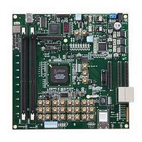
LFE3-95E-PCIE-DKN Lattice, LFE3-95E-PCIE-DKN Datasheet - Page 88

LFE3-95E-PCIE-DKN
Manufacturer Part Number
LFE3-95E-PCIE-DKN
Description
MCU, MPU & DSP Development Tools LatticeECP3 PCI Express Dev Kit
Manufacturer
Lattice
Datasheet
1.LFE3-150EA-7FN672CTW.pdf
(130 pages)
Specifications of LFE3-95E-PCIE-DKN
Processor To Be Evaluated
LFE3-95EA-x
Processor Series
LatticeECP3
Interface Type
SPI
Operating Supply Voltage
1.2 V to 3.3 V
Lead Free Status / RoHS Status
Lead free / RoHS Compliant
- Current page: 88 of 130
- Download datasheet (3Mb)
Lattice Semiconductor
SERDES/PCS Block Latency
Table 3-8 describes the latency of each functional block in the transmitter and receiver. Latency is given in parallel
clock cycles. Figure 3-12 shows the location of each block.
Table 3-8. SERDES/PCS Latency Breakdown
Figure 3-12. Transmitter and Receiver Latency Block Diagram
Transmit Data Latency
T1
T2
T3
T4
T5
Receive Data Latency
R1
R2
R3
R4
R5
R6
R7
1. 1 = -245ps, 2 = +88ps, 3 = +112ps.
2. 1 = +118ps, 2 = +132ps, 3 = +700ps.
Item
HDOUTPi
HDOUTNi
HDINPi
HDINNi
FPGA Bridge - Gearing disabled with different clocks
FPGA Bridge - Gearing disabled with same clocks
FPGA Bridge - Gearing enabled
8b10b Encoder
SERDES Bridge transmit
Serializer: 8-bit mode
Serializer: 10-bit mode
Pre-emphasis ON
Pre-emphasis OFF
Equalization ON
Equalization OFF
Deserializer: 8-bit mode
Deserializer: 10-bit mode
SERDES Bridge receive
Word alignment
8b10b decoder
Clock Tolerance Compensation
FPGA Bridge - Gearing disabled with different clocks
FPGA Bridge - Gearing disabled with same clocks
FPGA Bridge - Gearing enabled
Transmitter
Receiver
REFCLK
EQ
2
1
TX PLL
SERDES
REFCLK
CDR
Description
Serializer
8:1/10:1
Transmit Clock
T4
Deserializer
R1
1:8/1:10
SERDES Bridge
R2
BYPASS
Polarity
Adjust
BYPASS
Polarity
Adjust
T3
Recovered Clock
3-36
BYPASS
Min.
R3
WA
3.1
—
—
—
—
—
—
—
—
—
—
—
—
—
—
1
1
7
1
1
Encoder
BYPASS
BYPASS
DEC
PCS
Avg.
T2
DC and Switching Characteristics
15
—
—
—
—
—
—
—
—
—
—
—
—
—
—
—
3
3
3
3
R4
LatticeECP3 Family Data Sheet
BYPASS
Elastic
Buffer
FIFO
Max.
—
—
—
—
—
—
—
—
—
—
23
—
—
—
—
5
5
4
5
5
R5
FPGA Bridge
15 +
18 +
10 +
12 +
1 +
0 +
Fixed
—
—
—
—
—
Sample
2
2
3
2
1
1
3
Down
FIFO
Sample
1
2
R6
FIFO
Up
BYPASS
2
3
1
1
3
3
T1
Bypass
—
—
—
—
—
—
—
—
—
—
—
—
—
1
1
1
1
1
1
1
FPGA Core
FPGA
EBRD Clock
Receive Data
FPGA
Receive Clock
FPGA
Transmit Clock
Transmit Data
word clk
word clk
word clk
word clk
word clk
word clk
word clk
word clk
word clk
word clk
word clk
word clk
UI + ps
UI + ps
UI + ps
UI + ps
UI + ps
UI + ps
UI + ps
UI + ps
Units
Related parts for LFE3-95E-PCIE-DKN
Image
Part Number
Description
Manufacturer
Datasheet
Request
R

Part Number:
Description:
FPGA - Field Programmable Gate Array 92K LUTs, 490 I/O 8 Speed
Manufacturer:
Lattice

Part Number:
Description:
FPGA - Field Programmable Gate Array 92K LUTs, 380 I/O 7 Speed
Manufacturer:
Lattice

Part Number:
Description:
FPGA - Field Programmable Gate Array 92K LUTs, 295 I/O 7 Speed
Manufacturer:
Lattice

Part Number:
Description:
FPGA - Field Programmable Gate Array 92K LUTs, 380 I/O 6 Speed
Manufacturer:
Lattice

Part Number:
Description:
FPGA - Field Programmable Gate Array 92K LUTs, 490 I/O 6 Speed
Manufacturer:
Lattice

Part Number:
Description:
FPGA - Field Programmable Gate Array 92K LUTs, 295 I/O 8 Speed
Manufacturer:
Lattice

Part Number:
Description:
FPGA - Field Programmable Gate Array 92K LUTs, 490 I/O 8 Speed
Manufacturer:
Lattice

Part Number:
Description:
FPGA - Field Programmable Gate Array 92K LUTs, 380 I/O 8 Speed
Manufacturer:
Lattice

Part Number:
Description:
FPGA - Field Programmable Gate Array 92K LUTs, 490 I/O 6 Speed
Manufacturer:
Lattice

Part Number:
Description:
FPGA - Field Programmable Gate Array 92K LUTs, 295 I/O 6 Speed
Manufacturer:
Lattice

Part Number:
Description:
FPGA - Field Programmable Gate Array 92K LUTs, 490 I/O 7 Speed
Manufacturer:
Lattice

Part Number:
Description:
FPGA - Field Programmable Gate Array 92K LUTs, 295 I/O 8 Speed
Manufacturer:
Lattice

Part Number:
Description:
FPGA - Field Programmable Gate Array 92K LUTs, 490 I/O 7 Speed
Manufacturer:
Lattice

Part Number:
Description:
FPGA - Field Programmable Gate Array 92K LUTs, 380 I/O 6 Speed
Manufacturer:
Lattice

Part Number:
Description:
FPGA - Field Programmable Gate Array 92K LUTs, 295 I/O 7 Speed
Manufacturer:
Lattice


