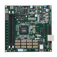
LFE3-95E-PCIE-DKN Lattice, LFE3-95E-PCIE-DKN Datasheet - Page 9

LFE3-95E-PCIE-DKN
Manufacturer Part Number
LFE3-95E-PCIE-DKN
Description
MCU, MPU & DSP Development Tools LatticeECP3 PCI Express Dev Kit
Manufacturer
Lattice
Datasheet
1.LFE3-150EA-7FN672CTW.pdf
(130 pages)
Specifications of LFE3-95E-PCIE-DKN
Processor To Be Evaluated
LFE3-95EA-x
Processor Series
LatticeECP3
Interface Type
SPI
Operating Supply Voltage
1.2 V to 3.3 V
Lead Free Status / RoHS Status
Lead free / RoHS Compliant
Architecture
Lattice Semiconductor
LatticeECP3 Family Data Sheet
ROM Mode
ROM mode uses the LUT logic; hence, Slices 0 through 3 can be used in ROM mode. Preloading is accomplished
through the programming interface during PFU configuration.
For more information, please refer to TN1179,
LatticeECP3 Memory Usage
Guide.
Routing
There are many resources provided in the LatticeECP3 devices to route signals individually or as busses with
related control signals. The routing resources consist of switching circuitry, buffers and metal interconnect (routing)
segments.
The LatticeECP3 family has an enhanced routing architecture that produces a compact design. The ispLEVER
design tool suite takes the output of the synthesis tool and places and routes the design.
sysCLOCK PLLs and DLLs
The sysCLOCK PLLs provide the ability to synthesize clock frequencies. All the devices in the LatticeECP3 family
support four to ten full-featured General Purpose PLLs.
General Purpose PLL
The architecture of the PLL is shown in Figure 2-4. A description of the PLL functionality follows.
CLKI is the reference frequency (generated either from the pin or from routing) for the PLL. CLKI feeds into the
Input Clock Divider block. The CLKFB is the feedback signal (generated from CLKOP, CLKOS or from a user clock
pin/logic). This signal feeds into the Feedback Divider. The Feedback Divider is used to multiply the reference fre-
quency.
Both the input path and feedback signals enter the Voltage Controlled Oscillator (VCO) block. In this block the dif-
ference between the input path and feedback signals is used to control the frequency and phase of the oscillator. A
LOCK signal is generated by the VCO to indicate that the VCO has locked onto the input clock signal. In dynamic
mode, the PLL may lose lock after a dynamic delay adjustment and not relock until the t
parameter has been
LOCK
satisfied.
The output of the VCO then enters the CLKOP divider. The CLKOP divider allows the VCO to operate at higher fre-
quencies than the clock output (CLKOP), thereby increasing the frequency range. The Phase/Duty Select block
adjusts the phase and duty cycle of the CLKOS signal. The phase/duty cycle setting can be pre-programmed or
dynamically adjusted. A secondary divider takes the CLKOP or CLKOS signal and uses it to derive lower frequency
outputs (CLKOK).
The primary output from the CLKOP divider (CLKOP) along with the outputs from the secondary dividers (CLKOK
and CLKOK2) and Phase/Duty select (CLKOS) are fed to the clock distribution network.
The PLL allows two methods for adjusting the phase of signal. The first is referred to as Fine Delay Adjustment.
This inserts up to 16 nominal 125ps delays to be applied to the secondary PLL output. The number of steps may
be set statically or from the FPGA logic. The second method is referred to as Coarse Phase Adjustment. This
allows the phase of the rising and falling edge of the secondary PLL output to be adjusted in 22.5 degree steps.
The number of steps may be set statically or from the FPGA logic.
2-6


