AD10242BZ Analog Devices Inc, AD10242BZ Datasheet
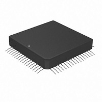
IC,A/D CONVERTER,DUAL,12-BIT,HYBRID,QFP,68PIN

AD10242BZ

Manufacturer Part Number
AD10242BZ
Description
IC,A/D CONVERTER,DUAL,12-BIT,HYBRID,QFP,68PIN
Manufacturer
Analog Devices Inc
Datasheet

Specifications of AD10242BZ

Rohs Status
RoHS non-compliant
Number Of Bits
12
Sampling Rate (per Second)
40M
Data Interface
Parallel
Number Of Converters
2
Power Dissipation (max)
2W
Voltage Supply Source
Analog and Digital, Dual ±
Operating Temperature
-40°C ~ 85°C
Mounting Type
Surface Mount
Package / Case
68-CLCC
For Use With
AD10242/PCB - KIT EVAL PCB FOR AD10242
Lead Free Status / RoHS Status

Available stocks

Company
Part Number
Manufacturer
Quantity
Price
Part Number:
AD10242BZ
Manufacturer:
NS
Quantity:
22
Part Number:
AD10242BZ
Manufacturer:
ADI
Quantity:
32
a
GENERAL DESCRIPTION
The AD10242 is a complete dual signal chain solution including
on-board amplifiers, references, ADCs, and output buffering
providing unsurpassed total system performance. Each channel is
laser trimmed for gain and offset matching and provides channel-
to-channel crosstalk performance better than 80 dB. The AD10242
utilizes two each of the AD9632, OP279, and AD9042 in a cus-
tom MCM to gain space, performance, and cost advantages over
solutions previously available.
REV. C
Information furnished by Analog Devices is believed to be accurate and
reliable. However, no responsibility is assumed by Analog Devices for its
use, nor for any infringements of patents or other rights of third parties that
may result from its use. No license is granted by implication or otherwise
under any patent or patent rights of Analog Devices. Trademarks and
registered trademarks are the property of their respective companies.
FEATURES
2 Matched ADCs with Input Signal Conditioning
Selectable Bipolar Input Voltage Range
Full MIL-STD-883B Compliant
80 dB Spurious-Free Dynamic Range
Trimmed Channel-Channel Matching
APPLICATIONS
Radar Processing
Communications Receivers
FLIR Processing
Secure Communications
Any I/Q Signal Processing Application
( 0.5 V,
(LSB) D0A
UCOM
UNEG
UPOS
D1A
D2A
D3A
D4A
D5A
D6A
D7A
D8A
1.0 V,
2.0 V)
A
ENC
IN
TIMING
3
9
OP279
ENC
OP279
A
OUTPUT BUFFERING
IN
D9A
2
V
D10A D11A
REF
12
A
IN
AD9632
AD9042
(MSB)
1
FUNCTIONAL BLOCK DIAGRAM
Dual, 12-Bit, 40 MSPS MCM A/D Converter
UNEG UCOM
with Analog Input Signal Conditioning
AD10242
UPOS
The AD10242 operates with ± 5.0 V for the analog signal condi-
tioning with a separate 5.0 V supply for the analog-to-digital
conversion. Each channel is completely independent, allowing
operation with independent encode or analog inputs. The AD10242
also offers the user a choice of analog input signal ranges to mini-
mize additional signal conditioning required for multiple functions
within a single system. The heart of the AD10242 is the AD9042,
which is designed specifically for applications requiring wide
dynamic range.
The AD10242 is manufactured on Analog Devices’
MIL-PRF-38534 MCM line and is completely qualified. Units
are packaged in a custom, cofired, ceramic 68-lead gull wing
package and specified for operation from –55°C to +125°C.
Contact the factory for additional custom options including those
that allow the user to ac couple the ADC directly, bypassing the
front end amplifier section. Also see the AD9042 data sheet for
additional details on ADC performance.
PRODUCT HIGHLIGHTS
1. Guaranteed sample rate of 40 MSPS.
2. Dynamic performance specified over entire Nyquist band;
3. Low power dissipation: <2 W off ± 5.0 V supplies.
4. User defined input amplitude.
5. Packaged in 68-lead ceramic leaded chip carrier.
One Technology Way, P.O. Box 9106, Norwood, MA 02062-9106, U.S.A.
Tel: 781/329-4700
Fax: 781/326-8703
spurious signals @ 80 dBc for –1 dBFS input signals.
(LSB)
D0B
OP279
D1B
A
IN
3
D2B
OP279
A
OUTPUT BUFFERING
AD9042
IN
D3B
© 2003 Analog Devices, Inc. All rights reserved.
2
V
D4B
REF
12
7
A
IN
AD9632
1
D5B
TIMING
D6B
5
AD10242
ENC
ENC
D11B (MSB)
D10B
D9B
D8B
D7B
www.analog.com

Related parts for AD10242BZ

AD10242BZ Summary of contents

Page 1

FEATURES 2 Matched ADCs with Input Signal Conditioning Selectable Bipolar Input Voltage Range ( 0.5 V, 1.0 V, 2.0 V) Full MIL-STD-883B Compliant 80 dB Spurious-Free Dynamic Range Trimmed Channel-Channel Matching APPLICATIONS Radar Processing Communications Receivers FLIR Processing Secure ...

Page 2

... V 25° Full 25° Full 25° Full –2– AD10242BZ/TZ Min Typ Max 12 Guaranteed ± 0.05 –0.5 +0.5 ± 1.0 –2.0 +2.0 ± 0.1 ± 0.5 –1.0 +1.0 ± 0.8 –1.5 +1.5 ± 0.1 ± 0.5 ± 1.0 ± 2 ...

Page 3

... Full IV 12 Full Full Full VI Full V Full VI Full V Full VI Full V Full Full Full Full IV 12 –3– AD10242 AD10242BZ/TZ Min Typ Max Unit 81 dBFS 70 80 dBFS 70 79 dBFS 63 70 dBFS 63 69 dBFS 60 67 dBFS 60 66 dBFS 70 76 dBc 0.3 1.0 LSB ...

Page 4

... JA tested at temperature extremes. ORDERING GUIDE Package Description 68-Lead Ceramic Leaded Chip Carrier 68- Lead Ceramic Leaded Chip Carrier 68-Lead Ceramic Leaded Chip Carrier 68- Lead Ceramic Leaded Chip Carrier Evaluation Board with AD10242BZ –4– Table I. Output Coding Base 10 Input 2047 + 0.0 V – ...

Page 5

GNDA GNDA UPOSA AV (LSB) D0A GNDA CONNECT Pin No. Mnemonic 1 SHIELD 2, 5, 9–11, 26–27 GNDA 3 UNEGA 4 UCOMA UPOSA 13 ...

Page 6

AD10242 DEFINITION OF SPECIFICATIONS Analog Bandwidth The analog input frequency at which the spectral power of the fundamental frequency (as determined by the FFT analysis) is reduced by 3 dB. Aperture Delay The delay between the 50% point of the ...

Page 7

1.0ns TYP A ENCODE t = 12ns TYP OD DIGITAL N – – OUTPUTS Figure 1. Timing Diagram EQUIVALENT CIRCUITS A 3 ...

Page 8

AD10242–Typical Performance Characteristics 0 –10 –20 –30 –40 –50 –60 –70 –80 –90 –100 FREQUENCY – MHz TPC 1. Single Tone @ 4.85 MHz 0 –10 –20 –30 –40 –50 –60 –70 –80 ...

Page 9

T = +25 C 65.0 64 +125 C 64.0 63.5 ENCODE = 40MSPS 63 62.5 62.0 61 ANALOG INPUT FREQUENCY – MHz TPC 7. SNR vs SFDR ...

Page 10

AD10242 SFDR (dBFS ENCODE = 40MSPS 29.2 ANALOG INPUT FREQUENCY – MHz TPC 13. SNR/Harmonics THEORY OF OPERATION Refer to the functional block diagram. ...

Page 11

If a logic threshold other than the nominal 1 required, the following equations show how to use an external resistor, Rx, to raise or lower the trip point (see Figure kΩ ...

Page 12

AD10242 USING THE FLEXIBLE INPUT The AD10242 has been designed with the user’s ease of opera- tion in mind. Multiple input configurations have been included on board to allow the user a choice of input signal levels and input impedance. ...

Page 13

SMA SMA 0 H2DM 8 J15 U1 OUT 1 K1115 AD9696KN 5VA H2DM R9 E5 J17 470 R10 C14 5 470 0.1 ...

Page 14

AD10242 Care should be taken when placing the digital output runs. Because the digital outputs have such a high slew rate, the capacitive loading on the digital outputs should be minimized. Circuit traces for the digital outputs should be kept ...

Page 15

DETAIL A TOE DOWN ANGLE 0–8 DEGREES 0.060 (1.52) 0.050 (1.27) 0.040 (1.02) CONTROLLING DIMENSIONS ARE IN INCHES; MILLIMETER DIMENSIONS (IN PARENTHESES) ARE ROUNDED-OFF INCH EQUIVALENTS FOR REFERENCE ONLY AND ARE NOT APPROPRIATE FOR ...

Page 16

–16– ...

Related keywords