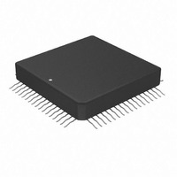
AD10242TZ Analog Devices Inc, AD10242TZ Datasheet - Page 4

AD10242TZ
Manufacturer Part Number
AD10242TZ
Description
IC,A/D CONVERTER,DUAL,12-BIT,HYBRID,QFP,68PIN
Manufacturer
Analog Devices Inc
Datasheet
1.AD10242BZ.pdf
(16 pages)
Specifications of AD10242TZ
Rohs Status
RoHS non-compliant
Number Of Bits
12
Sampling Rate (per Second)
40M
Data Interface
Parallel
Number Of Converters
2
Power Dissipation (max)
2W
Voltage Supply Source
Analog and Digital, Dual ±
Operating Temperature
-55°C ~ 125°C
Mounting Type
Surface Mount
Package / Case
68-CLCC
For Use With
AD10242/PCB - KIT EVAL PCB FOR AD10242
Lead Free Status / RoHS Status
Available stocks
Company
Part Number
Manufacturer
Quantity
Price
Part Number:
AD10242TZ
Manufacturer:
ADI/亚德诺
Quantity:
20 000
Company:
Part Number:
AD10242TZ/883
Manufacturer:
ZCOMM
Quantity:
1 400
AD10242
ABSOLUTE MAXIMUM RATINGS
Parameter
ELECTRICAL
ENVIRONMENTAL
NOTES
1
2
CAUTION
ESD (electrostatic discharge) sensitive device. Electrostatic charges as high as 4000 V readily
accumulate on the human body and test equipment and can discharge without detection. Although
the AD10242 features proprietary ESD protection circuitry, permanent damage may occur on
devices subjected to high energy electrostatic discharges. Therefore, proper ESD precautions are
recommended to avoid performance degradation or loss of functionality.
Absolute maximum ratings are limiting values to be applied individually, and beyond
which the serviceability of the circuit may be impaired. Functional operability is not
necessarily implied. Exposure to absolute maximum rating conditions for an
extended period of time may affect device reliability.
Typical thermal impedances for “Z” package: θ
V
V
Analog Input Voltage
Analog Input Current
Digital Input Voltage (ENCODE)
ENCODE, ENCODE Differential Voltage
Digital Output Current
Operating Temperature (Case)
Maximum Junction Temperature
Lead Temperature (Soldering, 10 sec)
Storage Temperature Range (Ambient)
CC
EE
Voltage
Voltage
M
AD10242BZ
AD10242TZ
AD10242TZ/883B
5962-9581501HXA
AD10242/PCB
odel
2
Temperature Range
–40°C to +85°C (Case)
–55°C to +125°C (Case)
–55°C to +125°C (Case)
–55°C to +125°C (Case)
25°C
JC
1
= 11°C/W; θ
Min
0
–7
V
–10
0
–40
–55
–65
EE
JA
= 30°C/W.
Max
7
0
V
+10
V
4
+40
+125 °C
175
300
+150 °C
CC
CC
ORDERING GUIDE
Unit
V
V
V
mA
V
V
mA
°C
°C
Package Description
68-Lead Ceramic Leaded Chip Carrier
68- Lead Ceramic Leaded Chip Carrier
68-Lead Ceramic Leaded Chip Carrier
68- Lead Ceramic Leaded Chip Carrier
Evaluation Board with AD10242BZ
–4–
MSB
0111111111111
0000000000001
0000000000000
1111111111111
1000000000000
EXPLANATION OF TEST LEVELS
Test Level
I
II – 100% production tested at 25°C, and sample tested at
III – Sample Tested Only.
IV – Parameter is guaranteed by design and characterization
V – Parameter is a typical value only.
VI – All devices are 100% production tested at 25°C; sample
– 100% Production Tested.
specified temperatures. AC testing done on sample basis.
testing.
tested at temperature extremes.
LSB
Table I. Output Coding
0
–1, 4095
–2047, 2048
Base 10
2047
+1
Package Option
Z-68A
Z-68A
Z-68A
Z-68A
WARNING!
ESD SENSITIVE DEVICE
Input
+FS
0.0 V
–FS
REV. C


