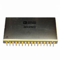
AD1380KD Analog Devices Inc, AD1380KD Datasheet

AD1380KD
Specifications of AD1380KD
Related parts for AD1380KD
AD1380KD Summary of contents
Page 1
... V, ±5 V, ± and +10 V. Important performance characteristics of the AD1380 include maximum linearity error of ±0.003% of FSR (AD1380KD) and maximum 16-bit conversion time of 14 μs. Transfer characteristics of the AD1380 (gain, offset and linearity) are specified for the combined ADC/sample-and-hold amplifier (SHA), so total performance is guaranteed as a system ...
Page 2
AD1380 TABLE OF CONTENTS Specifications..................................................................................... 3 Absolute Maximum Ratings............................................................ 5 ESD Caution.................................................................................. 5 Theory of Operation ........................................................................ 6 Description of Operation ................................................................ 7 Gain Adjustment .......................................................................... 7 Zero Offset Adjustment............................................................... 7 Timing............................................................................................ 7 REVISION HISTORY 6/05—Rev Rev. D ...
Page 3
... Bits) 5 1.1 +14.5 +15 +15.5 −14.5 −15 −15.5 +4.75 +5 +5. 900 Rev Page AD1380KD Min Typ Max 16 ±2.5 ±5 ± ±0.05 ±0.1 3 ±0.02 ±0.05 3 ±0.02 ±0.05 ±0.003 ±0.003 85 115 900 50 100 ...
Page 4
... Logic 0 = 0.8 V max; Logic 1 = 2.0 V min for inputs. Logic 0 = 0.4 V max; Logic 1 = 2.4 V min for digital outputs. 2 Tested on ±10 V and +10 V ranges. 3 Adjustable to zero. 4 Full-scale range. 5 Guaranteed but not 100% production tested. AD1380JD Min Typ Max −25 to +85 Rev Page AD1380KD Min Typ Max −25 to +85 Unit °C °C ...
Page 5
ABSOLUTE MAXIMUM RATINGS Table 2. Parameter Supply Voltage Logic Supply Voltage Analog Ground to Digital Ground Analog Inputs (Pin 6, Pin 7, Pin 31) Digital Input Output Short-Circuit Duration to Ground Sample/Hold Data Junction Temperature Storage Temperature Lead Temperature (Soldering, ...
Page 6
AD1380 THEORY OF OPERATION A 16-bit ADC partitions the range of analog inputs into 2 discrete ranges or quanta. All analog values within a given quantum are represented by the same digital code, usually assigned to the nominal midrange value. ...
Page 7
DESCRIPTION OF OPERATION On receipt of a CONVERT START command, the AD1380 converts the voltage at its analog input into an equivalent 16-bit binary number. This conversion is accomplished as follows: the 16-bit successive-approximation register (SAR) has its 16-bit outputs ...
Page 8
AD1380 DIGITAL OUTPUT DATA Parallel data from TTL storage registers is in negative true form (Logic and Logic 0 = 2.4 V). Parallel data output coding is complementary binary for unipolar ranges and comple- mentary offset ...
Page 9
CALIBRATION (14-BIT RESOLUTION EXAMPLES) External zero adjustment and gain adjustment potentiometers, connected as shown in Figure 3 and Figure 4, are used for device calibration. To prevent interaction of these two adjustments, zero is always adjusted first and then gain. ...
Page 10
AD1380 +15V 10kΩ 300kΩ TO 100kΩ GAIN ADJ –15V 0.01μF +15V + 1μF + 1μF –15V NOTE: ANALOG ( ) AND DIGITAL ( Figure 9. Analog and Power Connections for Unipolar Input Range +15V 10kΩ ...
Page 11
APPLICATIONS High performance sampling analog-to-digital converters like the AD1380 require dynamic characterization to ensure that they meet or exceed their desired performance parameters for signal processing applications. Key dynamic parameters include signal-to-noise ratio (SNR) and total harmonic distortion (THD), which ...
Page 12
... ORDERING GUIDE Model Max Linearity Error AD1380JD 0.006% FSR AD1380KD 0.003% FSR © 2005 Analog Devices, Inc. All rights reserved. Trademarks and registered trademarks are the property of their respective owners. C00764–0–6/05(D) 1.728 (43.89) MAX ...


