AD2S90AP Analog Devices Inc, AD2S90AP Datasheet
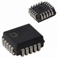
Resolver To Digital Converter IC

AD2S90AP

Manufacturer Part Number
AD2S90AP
Description
Resolver To Digital Converter IC
Manufacturer
Analog Devices Inc
Type
R/D Converterr
Datasheet

Specifications of AD2S90AP

Peak Reflow Compatible (260 C)
No
No. Of Bits
12 Bit
Leaded Process Compatible
No
Mounting Type
Surface Mount
Interface Type
Serial, Parallel
Package / Case
20-PLCC
Rohs Status
RoHS non-compliant
Input Type
Parallel
Output Type
Digital
Interface
Serial
Current - Supply
10mA
Lead Free Status / RoHS Status
Contains lead / RoHS non-compliant

Available stocks

Company
Part Number
Manufacturer
Quantity
Price
Part Number:
AD2S90AP
Manufacturer:
AD
Quantity:
5 510
Part Number:
AD2S90AP
Manufacturer:
Analog Devices Inc
Quantity:
10 000
Part Number:
AD2S90AP
Manufacturer:
ADI
Quantity:
128
Part Number:
AD2S90AP
Manufacturer:
ADI
Quantity:
8 000
Part Number:
AD2S90AP
Manufacturer:
ADI/亚德诺
Quantity:
20 000
Part Number:
AD2S90APZ
Manufacturer:
AD
Quantity:
5 510
Part Number:
AD2S90APZ
Manufacturer:
AD
Quantity:
1
Part Number:
AD2S90APZ
Manufacturer:
Analog Devices Inc
Quantity:
10 000
Part Number:
AD2S90APZ
Manufacturer:
ADI
Quantity:
128
a
GENERAL DESCRIPTION
The AD2S90 is a complete 12-bit resolution tracking resolver-
to-digital converter. No external components are required to
operate the device.
The converter accepts 2 V rms
3 kHz–20 kHz on the SIN, COS and REF inputs. A Type II
servo loop is employed to track the inputs and convert the input
SIN and COS information into a digital representation of the
input angle. The bandwidth of the converter is set internally at
1 kHz within the tolerances of the device. The guaranteed maxi-
mum tracking rate is 500 rps.
Angular position output information is available in two forms,
absolute serial binary and incremental A quad B.
The absolute serial binary output is 12-bit (1 in 4096). The data
output pin is high impedance when Chip Select CS is logic HI.
This allows the connection of multiple converters onto a com-
mon bus. Absolute angular information in serial pure binary
form is accessed by CS followed by the application of an exter-
nal clock (SCLK) with a maximum rate of 2 MHz.
The encoder emulation outputs A, B and NM continuously
produce signals equivalent to a 1024 line encoder. When de-
coded this corresponds to 12 bits of resolution. Three common
north marker pulsewidths are selected via a single pin (NMC).
An analog velocity output signal provides a representation of
velocity from a rotating resolver shaft traveling in either a clock-
wise or counterclockwise direction.
REV. D
Information furnished by Analog Devices is believed to be accurate and
reliable. However, no responsibility is assumed by Analog Devices for its
use, nor for any infringements of patents or other rights of third parties
which may result from its use. No license is granted by implication or
otherwise under any patent or patent rights of Analog Devices.
FEATURES
Complete Monolithic Resolver-to-Digital Converter
Incremental Encoder Emulation (1024-Line)
Absolute Serial Data (12-Bit)
Differential Inputs
12-Bit Resolution
Industrial Temperature Range
20-Lead PLCC
Low Power (50 mW)
APPLICATIONS
Industrial Motor Control
Servo Motor Control
Industrial Gauging
Encoder Emulation
Automotive Motion Sensing and Control
Factory Automation
Limit Switching
10% input signals in the range
The AD2S90 operates on 5 V dc
fabricated on Analog Devices’ Linear Compatible CMOS pro-
cess (LC
combines precision bipolar circuits with low power CMOS logic
circuits.
PRODUCT HIGHLIGHTS
Complete Resolver-Digital Interface. The AD2S90 provides
the complete solution for digitizing resolver signals (12-bit reso-
lution) without the need for external components.
Dual Format Position Data. Incremental encoder emulation
in standard A QUAD B format with selectable North Marker
width. Absolute serial 12-bit angular binary position data
accessed via simple 3-wire interface.
Single High Accuracy Grade in Low Cost Package. 10.6 arc
minutes of angular accuracy available in a 20-lead PLCC.
Low Power. Typically 50 mW power consumption.
One Technology Way, P.O. Box 9106, Norwood, MA 02062-9106, U.S.A.
Tel: 781/329-4700
Fax: 781/326-8703
COS LO
SIN LO
SCLK
DATA
NMC
COS
SIN
NM
Resolver-to-Digital Converter
CS
A
B
2
MOS). LC
Low Cost, Complete 12-Bit
DECODE
ANGLE
FUNCTIONAL BLOCK DIAGRAM
LOGIC
HIGH ACCURACY
SERIAL INTERFACE
2
World Wide Web Site: http://www.analog.com
MULTIPLIER
MOS is a mixed technology process that
SIN COS
UP-DOWN
COUNTER
ANGLE
DIGITAL
LATCH
SIN ( –
U/D
CLK
AMPLIFIER
5% power supplies and is
ERROR
© Analog Devices, Inc., 1999
)
RANGE V.C.O.
FREQUENCY
AD2S90
P.S.D. AND
DYNAMIC
SHAPING
HIGH
REF
VEL
DIR
CLKOUT

Related parts for AD2S90AP

AD2S90AP Summary of contents

Page 1

FEATURES Complete Monolithic Resolver-to-Digital Converter Incremental Encoder Emulation (1024-Line) Absolute Serial Data (12-Bit) Differential Inputs 12-Bit Resolution Industrial Temperature Range 20-Lead PLCC Low Power (50 mW) APPLICATIONS Industrial Motor Control Servo Motor Control Industrial Gauging Encoder Emulation Automotive Motion ...

Page 2

AD2S90–SPECIFICATIONS Parameter SIGNAL INPUTS Voltage Amplitude Frequency Input Bias Current Input Impedance 1 Common-Mode Volts CMRR REFERENCE INPUT Voltage Amplitude Frequency Input Bias Current Input Impedance Permissible Phase Shift CONVERTER DYNAMICS Bandwidth Maximum Tracking Rate Maximum VCO Rate (CLKOUT) Settling ...

Page 3

TIMING CHARACTERISTICS CSB SCLK DATA NOTES 1 Timing data are not 100% production tested. Sample tested at +25 C only to ensure conformance to data sheet limits. Logic output timing tests carried out using 10 pF, 100 k load. 2 ...

Page 4

... Exposure to absolute maximum rating conditions for extended periods may affect device reliability. ORDERING GUIDE Model Temperature Range Accuracy AD2S90AP – +85 C 10.6 arc min P-20A PIN CONFIGURATION ...

Page 5

... For a more detailed description of the output formats available see the Position Output section. OSCILLATOR REF COS COS 1 AGND 2 SIN 3 SIN LO AD2S90AP POWER RETURN Figure 5. Connecting the AD2S90 to a Resolver –5– AD2S90 0 90 180 270 = + – Pin 12. Reversal of these power 10%. The AD2S90 , NMC will select standard ...

Page 6

AD2S90 ABSOLUTE POSITION OUTPUT SERIAL INTERFACE Absolute angular position is represented by serial binary data and is extracted via a three-wire interface, DATA, CS and SCLK. The DATA output is held in a high impedance state when CS is HI. ...

Page 7

VELOCITY OUTPUT The analog velocity output VEL is scaled to produce 150 rps/V dc 15%. The sense is positive V dc for increasing angular rotation. VEL can drive a maximum load combination and 30 pF. The internal ...

Page 8

AD2S90 TMS32020 Interfacing Figure 11 shows the serial interface between the AD2S90 and the TMS32020. The interface is configured in alternate internal framing, external clock (externally inverted) mode. Sixteen bits of data are clocked from the AD2S90 into the data ...

Page 9

REMOTE MULTIPLE SENSOR INTERFACING The DATA output of the AD2S90 is held in a high impedance state until CS is taken LO. This allows a user to operate the AD2S90 in an application with more than one converter con- nected ...

Page 10

AD2S90 The small step response is given in Figure 20, and is the time taken for the converter to settle to within 1 LSB 7.00 ms (maximum) The large step response (steps >20 ) applies when the error ...

Page 11

AD2S90/AD2S99 TYPICAL CONFIGURATION Figure 21 shows a typical circuit configuration for the AD2S99 Oscillator and the AD2S90 Resolver-to-Digital Converter. The maximum level of the SIN and COS input signals to the AD2S90 should rms 10%. All the ...

Page 12

AD2S90 0.048 (1.21) 0.042 (1.07) OUTLINE DIMENSIONS Dimensions shown in inches and (mm). P-20A 20-Lead Plastic Leaded Chip Carrier (PLCC) 0.180 (4.57) 0.165 (4.19) 0.048 (1.21) 0.056 (1.42) 0.042 (1.07) 0.025 (0.63) 0.042 (1.07) 0.015 (0.38 0.021 (0.53) ...

Related keywords