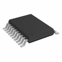
AD5330BRUZ-REEL Analog Devices Inc, AD5330BRUZ-REEL Datasheet - Page 21

AD5330BRUZ-REEL
Manufacturer Part Number
AD5330BRUZ-REEL
Description
IC,D/A CONVERTER,SINGLE,8-BIT,CMOS,SSOP,20PIN
Manufacturer
Analog Devices Inc
Datasheet
1.AD5331BRUZ.pdf
(28 pages)
Specifications of AD5330BRUZ-REEL
Settling Time
6µs
Number Of Bits
8
Data Interface
Parallel
Number Of Converters
1
Voltage Supply Source
Single Supply
Power Dissipation (max)
1.25mW
Operating Temperature
-40°C ~ 105°C
Mounting Type
Surface Mount
Package / Case
20-TSSOP
Lead Free Status / RoHS Status
Lead free / RoHS Compliant
Available stocks
Company
Part Number
Manufacturer
Quantity
Price
Company:
Part Number:
AD5330BRUZ-REEL7
Manufacturer:
ATMEL
Quantity:
2 804
Part Number:
AD5330BRUZ-REEL7
Manufacturer:
ADI/亚德诺
Quantity:
20 000
APPLICATIONS INFORMATION
TYPICAL APPLICATION CIRCUITS
The AD5330/AD5331/AD5340/AD5341 can be used with
a wide range of reference voltages, especially if the reference
inputs are configured to be unbuffered, in which case the
devices offer full, one-quadrant multiplying capability over a
reference range of 0.25 V to V
can be used with a fixed, precision reference voltage. Figure 43
shows a typical setup for the devices when using an external
reference connected to the unbuffered reference inputs. If the
reference inputs are unbuffered, the reference input range is
from 0.25 V to V
used, the reference range is reduced. Suitable references for 5 V
operation are the
suitable external reference is the AD589, a 1.23 V band gap
reference.
DRIVING V
If an output range of 0 V to V
solution is to connect the reference inputs to V
supply may not be very accurate and may be noisy, the devices
can be powered from the reference voltage, for example using
a 5 V reference such as the ADP667, as shown in Figure 44.
AD589 WITH V
Figure 43. AD5330/AD5331/AD5340/AD5341 Using External Reference
AD780/REF192
WITH V
VSET
EXT
REF
6V TO 16V
ADP667
Figure 44. Using an ADP667 as Power and Reference to
GND
V
OR
GND SHDN
IN
V
DD
IN
V
DD
DD
= 5V
OUT
V
= 2.5V
0.1µF
FROM THE REFERENCE VOLTAGE
OUT
DD
AD780
AD5330/AD5331/AD5340/AD5341
, but if the on-chip reference buffers are
0.1µF
+
0.1µF
and REF192. For 2.5 V operation, a
10µF
DD
DD
V
V
DD
REF
. More typically, these devices
is required, the simplest
V
AD5330/AD5331/
AD5340/AD5341
REF
+
10µF
AD5330/AD5331/
AD5340/AD5341
V
DD
GND
= 2.5V TO 5.5V
GND
V
DD
DD
V
OUT
. Because this
V
OUT
Rev. A | Page 21 of 28
BIPOLAR OPERATION USING THE AD5330/AD5331/
AD5340/AD5341
The AD5330/AD5331/AD5340/AD5341 are designed for
single-supply operation, but bipolar operation is achievable
using the circuit shown in Figure 45. The circuit shown has
been configured to achieve an output voltage range of –5 V <
V
achievable using an
The output voltage for any input code can be calculated as follows:
where:
D is the decimal equivalent of the code loaded to the DAC.
N is the DAC resolution.
V
with:
DECODING MULTIPLE AD5330/AD5331/
AD5340/AD5341
The CS pin on these devices can be used in applications to
decode a number of DACs. In this application, all DACs in the
system receive the same data and WR pulses, but only CS to one
of the DACs is active at any one time, so data is only written to
the DAC whose CS is low. If multiple AD5341s are being used, a
common HBEN line is also required to determine if the data is
written to the high byte or low byte register of the selected DAC.
The 74HC139 is used as a 2-line to 4-line decoder to address
any of the DACs in the system. To prevent timing errors, the
enable input should be brought to its inactive state while the
coded address inputs are changing state. Figure 46 shows a
diagram of a typical setup for decoding multiple devices in a
system. Once data has been written sequentially to all DACs in
AD589 WITH V
Figure 45. Bipolar Operation using the AD5330/AD5331/AD5340/AD5341
REF
O
V
R1 = R3 = 10 kΩ.
R2 = R4 = 20 kΩ and V
V
EXT
REF
AD780/REF192
WITH V
< +5 V. Rail-to-rail operation at the amplifier output is
REF
O
is the reference voltage input.
V
R4 × V
= (10 × D/2
O
GND
V
= 2.5 V.
OR
= [(1 + R4 / R3 ) × ( R2 /( R1 + R2 ) × (2 × V
IN
DD
V
DD
= 5V
OUT
AD5330/AD5331/AD5340/AD5341
REF
= 2.5V
/ R3
0.1µF
N
0.1µF
) − 5.
AD820
AD5330/AD5331/
AD5340/AD5341
+
V
10µF
REF
DD
or
= 5 V.
V
DD
OP295
GND
V
DD
= 5V
V
10kΩ
R3
OUT
as the output amplifier.
10kΩ
R1
R2
20kΩ
20kΩ
R4
REF
+5V
–5V
× D /2
N
V
)] –
O
= ±5V


