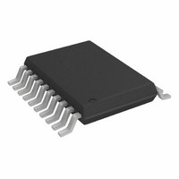
AD5330BRUZ-REEL Analog Devices Inc, AD5330BRUZ-REEL Datasheet - Page 4

AD5330BRUZ-REEL
Manufacturer Part Number
AD5330BRUZ-REEL
Description
IC,D/A CONVERTER,SINGLE,8-BIT,CMOS,SSOP,20PIN
Manufacturer
Analog Devices Inc
Datasheet
1.AD5331BRUZ.pdf
(28 pages)
Specifications of AD5330BRUZ-REEL
Settling Time
6µs
Number Of Bits
8
Data Interface
Parallel
Number Of Converters
1
Voltage Supply Source
Single Supply
Power Dissipation (max)
1.25mW
Operating Temperature
-40°C ~ 105°C
Mounting Type
Surface Mount
Package / Case
20-TSSOP
Lead Free Status / RoHS Status
Lead free / RoHS Compliant
Available stocks
Company
Part Number
Manufacturer
Quantity
Price
Company:
Part Number:
AD5330BRUZ-REEL7
Manufacturer:
ATMEL
Quantity:
2 804
Part Number:
AD5330BRUZ-REEL7
Manufacturer:
ADI/亚德诺
Quantity:
20 000
AD5330/AD5331/AD5340/AD5341
Parameter
POWER REQUIREMENTS
1
2
3
4
5
6
7
AC CHARACTERISTICS
V
Table 2.
Parameter
Output Voltage Settling Time
Slew Rate
Major Code Transition Glitch Energy
Digital Feedthrough
Multiplying Bandwidth
Total Harmonic Distortion
1
2
3
See the Terminology section.
Temperature range: B Version: −40°C to +105°C; typical specifications are at 25°C.
Linearity is tested using a reduced code range: AD5330 (Code 8 to Code 255); AD5331 (Code 28 to Code 1023); AD5340/AD5341 (Code 115 to Code 4095).
DC specifications tested with output unloaded.
This corresponds to x codes. x = deadband voltage/LSB size.
Guaranteed by design and characterization, not production tested.
For the amplifier output to reach its minimum voltage, offset error must be negative. For the amplifier output to reach its maximum voltage, V
gain error must be positive.
Guaranteed by design and characterization, not production tested.
See the Terminology section.
Temperature range: B Version: −40°C to +105°C; typical specifications are at 25°C.
DD
V
I
I
AD5330
AD5331
AD5340
AD5341
DD
DD
DD
= 2.5 V to 5.5 V. R
V
V
V
V
(Normal Mode)
(Power-Down Mode)
DD
DD
DD
DD
= 4.5 V to 5.5 V
= 2.5 V to 3.6 V
= 4.5 V to 5.5 V
= 2.5 V to 3.6 V
1
2
L
= 2 kΩ to GND, C
1
Min
2.5
Min
L
= 200 pF to GND; all specifications T
Typ
140
115
0.2
0.08
B Version
B Version
Typ
6
7
8
8
0.7
6
0.5
200
−70
2
3
Max
8
9
10
10
Max
5.5
250
200
1
1
Rev. A | Page 4 of 28
Unit
μs
μs
μs
μs
V/μs
nV/s
nV/s
kHz
dB
Unit
V
μA
μA
μA
μA
Conditions/Comments
V
¼ scale to ¾ scale change (0x40 to 0xC0)
¼ scale to ¾ scale change (0x100 to 0x300)
¼ scale to ¾ scale change (0x400 to 0xC00)
¼ scale to ¾ scale change (0x400 to 0xC00)
1 LSB change around major carry
V
V
REF
REF
REF
= 2 V; see Figure 29
= 2 V ± 0.1 V p-p; unbuffered mode
= 2.5 V ± 0.1 V p-p; frequency = 10 kHz
MIN
Conditions/Comments
DACs active and excluding load currents. Unbuffered
Reference, V
I
In buffered mode, extra current is (5 + V
where R
to T
DD
increases by 50 μA at V
MAX
, unless otherwise noted.
DAC
is the resistance of the resistor string.
IH
= V
DD
, V
IL
= GND
REF
> V
DD
− 100 mV.
REF
= V
REF
DD
/R
and offset plus
DAC
) μA,


