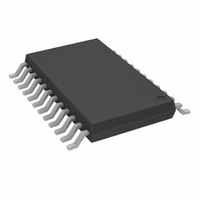
AD5335BRUZ Analog Devices Inc, AD5335BRUZ Datasheet - Page 2

AD5335BRUZ
Manufacturer Part Number
AD5335BRUZ
Description
10-BIT,QUAD BYTE DAC, I.C
Manufacturer
Analog Devices Inc
Datasheet
1.AD5336BRUZ.pdf
(20 pages)
Specifications of AD5335BRUZ
Settling Time
7µs
Number Of Bits
10
Data Interface
Parallel
Number Of Converters
4
Voltage Supply Source
Single Supply
Power Dissipation (max)
4.5mW
Operating Temperature
-40°C ~ 105°C
Mounting Type
Surface Mount
Package / Case
24-TSSOP
Number Of Channels
4
Resolution
10b
Conversion Rate
143KSPS
Interface Type
Parallel
Single Supply Voltage (typ)
3.3/5V
Dual Supply Voltage (typ)
Not RequiredV
Architecture
Resistor-String
Power Supply Requirement
Single
Output Type
Voltage
Integral Nonlinearity Error
±4LSB
Single Supply Voltage (min)
2.5V
Single Supply Voltage (max)
5.5V
Dual Supply Voltage (min)
Not RequiredV
Dual Supply Voltage (max)
Not RequiredV
Operating Temp Range
-40C to 105C
Operating Temperature Classification
Industrial
Mounting
Surface Mount
Pin Count
24
Package Type
TSSOP
Lead Free Status / RoHS Status
Lead free / RoHS Compliant
Lead Free Status / RoHS Status
Lead free / RoHS Compliant
Available stocks
Company
Part Number
Manufacturer
Quantity
Price
Company:
Part Number:
AD5335BRUZ
Manufacturer:
Analog Devices Inc
Quantity:
135
Part Number:
AD5335BRUZ
Manufacturer:
ADI/亚德诺
Quantity:
20 000
AD5334/AD5335/AD5336/AD5344–SPECIFICATIONS
Parameter
DC PERFORMANCE
DAC REFERENCE INPUT
OUTPUT CHARACTERISTICS
LOGIC INPUTS
POWER REQUIREMENTS
NOTES
1
2
3
4
5
6
7
Specifications subject to change without notice.
(V
See Terminology section.
Temperature range: B Version: –40°C to +105°C; typical specifications are at 25°C.
Linearity is tested using a reduced code range: AD5334 (Code 8 to 255); AD5335/AD5336 (Code 28 to 1023); AD5344 (Code 115 to 4095).
DC specifications tested with outputs unloaded.
This corresponds to x codes. x = Deadband voltage/LSB size.
Guaranteed by design and characterization, not production tested.
In order for the amplifier output to reach its minimum voltage, Offset Error must be negative. In order for the amplifier output to reach its maximum voltage, V
“Offset plus Gain” Error must be positive.
DD
AD5334
AD5335/AD5336
AD5344
Offset Error
Gain Error
Lower Deadband
Upper Deadband
Offset Error Drift
Gain Error Drift
DC Power Supply Rejection Ratio
DC Crosstalk
V
V
Reference Feedthrough
Channel-to-Channel Isolation
Minimum Output Voltage
Maximum Output Voltage
DC Output Impedance
Short Circuit Current
Power-Up Time
Input Current
V
V
Pin Capacitance
V
I
I
DD
DD
REF
REF
IL
IH
DD
= 2.5 V to 5.5 V, V
Resolution
Relative Accuracy
Differential Nonlinearity
Resolution
Relative Accuracy
Differential Nonlinearity
Resolution
Relative Accuracy
Differential Nonlinearity
V
V
V
V
, Input Low Voltage
, Input High Voltage
(Normal Mode)
(Power-Down Mode)
DD
DD
DD
DD
Input Range
Input Impedance
= 4.5 V to 5.5 V
= 2.5 V to 3.6 V
= 4.5 V to 5.5 V
= 2.5 V to 3.6 V
1
6
6
6
5
6
3, 4
REF
4, 7
6
4, 7
= 2 V. R
6
6
L
= 2 k
Min
0.25
2.4
2.1
2.0
2.5
to GND; C
B Version
Typ
8
± 0.15
± 0.02
10
± 0.5
± 0.05
12
± 2
± 0.2
± 0.4
± 0.1
10
10
–12
–5
–60
200
180
90
90
45
–90
–90
0.001
V
0.5
50
20
2.5
5
± 1
3.5
600
500
0.2
0.08
DD
– 0.001
L
=200 pF to GND; all specifications T
2
Max
± 1
± 0.25
± 4
± 0.5
± 16
± 1
± 3
± 1
60
60
V
0.8
0.6
0.5
5.5
900
700
1
1
DD
–2–
Unit
Bits
LSB
LSB
Bits
LSB
LSB
Bits
LSB
LSB
% of FSR
% of FSR
mV
ppm of FSR/°C
ppm of FSR/°C
dB
µV
V
kΩ
kΩ
kΩ
kΩ
dB
dB
V min
V max
Ω
mA
mA
µs
µs
µA
V
V
V
V
V
V
pF
V
µA
µA
µA
µA
mV
Conditions/Comments
Guaranteed Monotonic By Design Over All Codes
Guaranteed Monotonic By Design Over All Codes
Guaranteed Monotonic By Design Over All Codes
Lower Deadband Exists Only if Offset Error Is Negative
V
∆V
R
Gain = 0
Gain = 1. Input Impedance = R
Gain = 2. Input Impedance = R
Gain = 1. Input Impedance = R
Gain = 2. Input Impedance = R
Frequency = 10 kHz
Frequency = 10 kHz
Rail-to-Rail Operation
V
V
Coming Out of Power-Down Mode. V
Coming Out of Power-Down Mode. V
V
V
V
V
V
V
All DACs active and excluding load currents.
V
I
DD
MIN
DD
L
DD
DD
DD
DD
DD
DD
DD
DD
IH
DD
= 2 kΩ to GND, 2 kΩ to V
increases by 50 µA at V
= V
= 5 V ± 10%
= 5 V. Upper Deadband Exists Only if V
= 5 V
= 3 V
= 3 V ± 10%
= 2.5 V
= 5 V ± 10%
= 3 V ± 10%
= 2.5 V
to T
= ± 10%
DD
MAX
, V
unless otherwise noted.)
IL
= GND.
REF
DD
> V
DAC
DAC
DAC
DAC
; C
DD
L
(AD5336)
(AD5334)
(AD5336/AD5344)
(AD5334/AD5335)
= 200 pF to GND;
– 100 mV.
DD
DD
= 5 V
= 3 V
REF
= V
REF =
DD
REV. 0
V
and
DD


