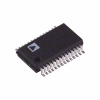
AD5725BRSZ-500RL7 Analog Devices Inc, AD5725BRSZ-500RL7 Datasheet

AD5725BRSZ-500RL7
Specifications of AD5725BRSZ-500RL7
AD5725BRSZ-500RL7TR
Available stocks
Related parts for AD5725BRSZ-500RL7
AD5725BRSZ-500RL7 Summary of contents
Page 1
FEATURES + ±15 V operation Unipolar or bipolar operation ±0.5 LSB max INL error, ±1 LSB max DNL error Settling time: 10 μs max (10 V step) Double-buffered inputs Simultaneous updating via LDAC Asynchronous CLR to zero/mid scale ...
Page 2
AD5725 TABLE OF CONTENTS Features .............................................................................................. 1 Applications ....................................................................................... 1 Functional Block Diagram .............................................................. 1 General Description ......................................................................... 1 Revision History ............................................................................... 2 Specifications ..................................................................................... 3 AC Performance Characteristics ................................................ 5 , Timing Characteristics ............................................................... 6 Absolute Maximum Ratings ............................................................ ...
Page 3
SPECIFICATIONS −15 V, DGND = Table 1. Parameter ACCURACY Resolution Relative Accuracy (INL) Differential Nonlinearity (DNL) Zero-Scale Error 2 Zero-Scale TC Full-Scale Error 2 Full-Scale TC REFERENCE INPUT V ...
Page 4
AD5725 −5 V/0 V, DGND = otherwise noted. Table 2. Parameter ACCURACY Resolution Relative Accuracy (INL) Differential Nonlinearity (DNL) Zero-Scale Error 2 Zero-Scale TC Full-Scale Error Full-Scale TC 2 ...
Page 5
AC PERFORMANCE CHARACTERISTICS AV = +15 V/+ −15 V/−5 V/0 V, DGND = unless otherwise noted. MIN MAX Table 3. Parameter DYNAMIC PERFORMANCE Output Voltage Settling Time Slew ...
Page 6
AD5725 1, 2 TIMING CHARACTERISTICS V/+ −5 V/0 V/−15 V, DGND = unless otherwise noted. MIN MAX Table 4. Parameter Limit ...
Page 7
Timing Diagrams t RCS RDS R A0/ HIGH-Z DATA DATA VALID OUT t CSD Figure 2. Data Read Timing t WCS R ...
Page 8
AD5725 ABSOLUTE MAXIMUM RATINGS T = 25°C unless otherwise noted. Transient currents 100 mA do not cause SCR latch-up. Table 5. Parameter AV to DGND DGND ...
Page 9
PIN CONFIGURATION AND FUNCTION DESCRIPTIONS Table 6. Pin Function Descriptions Pin No. Mnemonic Description 1 V Positive DAC Reference Input. The voltage applied to this pin defines the full-scale output voltage. REFP Allowable range Buffered Analog ...
Page 10
AD5725 TYPICAL PERFORMANCE CHARACTERISTICS 1 +15V –15V 0 –10V REFN T = 25°C 0.6 A 0.4 0.2 0 –0.2 –0.4 –0.6 –0.8 –1 (V) REFP Figure 7. ...
Page 11
AV = +15V –15V SS –0 +10V REFP V = –10V REFN T = 25°C A –0.3 0 500 1000 1500 2000 2500 3000 DAC (Code) Figure 13. Channel-to-Channel Matching ...
Page 12
AD5725 +15V –15V +10V REFP –10V REFN T = 25° 0.01 0.1 1 LOAD RESISTANCE (kΩ) Figure 19. Output Voltage Swing vs. ...
Page 13
AV = +15V V = +10V T = 25°C DD REFP –15V V = –10V BW = 100kHz SS REFN 1 CH1 50µ Figure 25. Broadband Noise 1.0 0.8 0.6 0.4 0.2 0 –0.2 –0.4 ...
Page 14
AD5725 TERMINOLOGY Relative Accuracy or Integral Nonlinearity (INL) For the DAC, relative accuracy or integral nonlinearity is a measure of the maximum deviation, in LSBs, from a straight line passing through the endpoints of the DAC transfer function. A typical ...
Page 15
THEORY OF OPERATION The AD5725 is a quad voltage output, 12-bit parallel input DAC featuring a 12-bit data bus with readback capability. The AD5725 operates from single or dual supplies ranging from + ±15 V. The output ...
Page 16
AD5725 Table 7. AD5725 Logic Truth Table A1 A0 R/W CS CLR Low Low Low Low High Low High Low Low High High Low Low Low High High High Low Low High Low Low Low Low High Low High Low ...
Page 17
POWER SUPPLIES Power supplies required are supply can be set between −15 V and supply; its operating range is between +5 V and + the digital output supply voltage ...
Page 18
AD5725 Figure 29 shows the AD5725 configured for − operation. An ADR01 and OP1177 are configured to produce a −10 V output, which is connected directly to V reference voltage. +15V V +15V IN ADR01 AV ...
Page 19
... AD5725ARSZ-500RL7 −40°C to +85°C AD5725ARSZ-REEL 1 −40°C to +85°C 1 AD5725BRSZ-1500RL7 −40°C to +85°C 1 AD5725BRSZ-1REEL −40°C to +85°C 1 AD5725BRSZ-500RL7 −40°C to +85°C 1 AD5725BRSZ-REEL −40°C to +85° RoHS Compliant Part. 10.50 10.20 9. 5.60 5.30 8 ...
Page 20
AD5725 NOTES ©2007–2008 Analog Devices, Inc. All rights reserved. Trademarks and registered trademarks are the property of their respective owners. D06442-0-12/08(A) Rev Page ...


