AD6635BB Analog Devices Inc, AD6635BB Datasheet
AD6635BB
Specifications of AD6635BB
Available stocks


Related parts for AD6635BB


AD6635BB Summary of contents
Page 1
FEATURES Four 80 MSPS Wideband Inputs (14 Linear Bits Plus 3 RSSI) 4 Real Input Ports/2 Complex Input Ports Processes 4 Wideband Channels (UMTS or cdma2000 1x GSM/EDGE, IS136 Channels 8 Independent Digital Receivers in a Single Package ...
Page 2
AD6635 GENERAL DESCRIPTION The AD6635 is a multimode, 8-channel, digital Receive Signal Processor (RSP) capable of processing up to four WCDMA channels. Each channel consists of four cascaded signal-process- ing elements: a frequency translator, two CIC decimating filters, and a ...
Page 3
TABLE OF CONTENTS FEATURES . . . . . . . . . . . . . . . . . . . . . . . . . . . . . . . . . . . . ...
Page 4
AD6635 TABLE OF CONTENTS 0x08: Port A Control Register . . . . . . . . . . . . . . . . . . . . . 50 0x09: Port B Control Register . . . . ...
Page 5
ARCHITECTURE Each channel of the AD6635 has four signal processing stages: a Frequency Translator, a second-order Resampling Cascaded Integrator Comb FIR Filter (rCIC2), a fifth-order Cascaded Integrator Comb FIR Filter (CIC5), and a RAM Coefficient FIR Filter (RCF). Multiple modes ...
Page 6
AD6635 SIGNAL OF INTEREST “IMAGE” – /2 –3 /8 –5 /16 – AFTER FREQUENCY TRANSLATION – /2 –3 /8 –5 /16 – ...
Page 7
... Full IV 2.4 Full IV Full IV 25∞C V 25∞C V Full Full IV –7– AD6635 AD6635BB Typ Max Unit 2.5 2.75 V 3.3 3.6 V ∞C +25 +85 AD6635BB Typ Max Unit 3.3 V CMOS 5 VDD – 0.2 V 0.2 0.4 V 880 mA 150 mA 485 830 mA 120 mA 2 ...
Page 8
... IV Full IV Full I Full IV Full IV Full IV Full IV Full IV 2 Full IV Full IV Full IV Full IV Full IV 3 Full Full I Full IV Full IV –8– AD6635BB Min Typ Max Unit 12.5 ns 5.6 0 CLK 5.6 0 CLK 30.0 ns 2.0 ns 1.0 ns 3.3 10.0 ns 2 3.0 ns 3.0 ns 1 ...
Page 9
... The timing parameters for Px[15:0], PxREQ, PxACK, LxCLKOUT, and Lx[7:0] apply for output ports and D. (x stands for D.) Specifications subject to change without notice. REV Test Temp Level 3 Full IV Full IV Full IV Full IV –9– AD6635 AD6635BB Min Typ Max Unit 1.0 ns 1 2.2 ...
Page 10
... All Timing Specifications valid over VDD range of 2. 2.75 V, and VDDIO range all outputs unless otherwise specified. LOAD Specification pertains to control signals: R/W, (WR), DS, (RD), CS0, CS1. 3 Specifications subject to change without notice Test AD6635BB Temp Level Min Typ Full IV 2.0 Full IV 2 ...
Page 11
... Model Temperature Range AD6635BB –40ºC to +85ºC AD6635BB/PCB CAUTION ESD (electrostatic discharge) sensitive device. Electrostatic charges as high as 4000 V readily accumulate on the human body and test equipment and can discharge without detection. Although the AD6635 features proprietary ESD protection circuitry, permanent damage may occur on devices subjected to high energy electrostatic discharges ...
Page 12
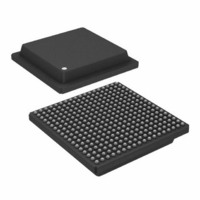
AD6635 PIN CONFIGURATION 2 19mm 19mm – 18 BALL ZAPHOD PACKAGE 1.00 BSC 1.00 BOTTOM VIEW BSC –12– A1 BALL CORNER ...
Page 13
A IENC INC0 INC12 INC7 VDDIO CLK0 INC1 INC8 INC11 B (Reserved) VDDIO C CLK1 PAREQ INC2 INC9 (Reserved) D CHIP0_ID0 LID-A PAACK INC3 CHIP0_ID1 CHIP0_ID2 INC4 E PAIQ VDD F SCLK0 VDD PCLK0 SDI0 ...
Page 14
AD6635 Name Type POWER SUPPLY VDD P VDDIO P GND G INPUTS 1 INA[13: EXPA[2: IENA I 1 INB[13: EXPB[2: IENB I 1 INC[13: EXPC[2: IENC I 1 ...
Page 15
Name Type MICROPORT CONTROL D[7:0] I/O/T A[2: (RD) I DTACK (RDY) 2 O/T R/W (WR) I MODE I CS0 1 I CS1 1 I SERIAL PORT CONTROL 1 SDI0 I 1 SCLK0 I 1 SDI4 I 1 SCLK4 ...
Page 16
AD6635 TIMING DIAGRAMS Figure 3. Level Indicator Output Switching Characteristics ( and (For and and for ...
Page 17
INx[13:0] EXPx[2:0] SYNCA SYNCB SYNCC SYNCD CLKn PCLKn Figure 9. PCLKn to CLKn Switching Characteristics Divide by 1 CLKn PCLKn Figure 10. PCLKn to CLKn Switching Characteristics Divide REV. 0 CLKn ...
Page 18
AD6635 PCLKn PxACK Figure 11. Master Mode PxACK to PCLKn Setup and Hold Characteristics ( and and PCLKn PxREQ t SPA PxACK Px[15:0] Figure 12. Master ...
Page 19
PCLKn PxACK Figure 14. Slave Mode PxACK to PCLKn Setup and Hold Characteristics ( and and PCLKn PxREQ t SPA PxACK Px[15:0] Figure 15. Slave Mode ...
Page 20
AD6635 PCLKn LxCLKOUT Figure 17. LxCLKOUT to PCLKn ( and and Switching Characteristics LxCLKOUT WAIT > 6 CYCLES ONE TIME CONNECTIVITY CHECK LxCLKIN Lx[7:0] Figure 18. ...
Page 21
TIMING DIAGRAMS – INM Microport Mode (MODE = 0) CLK0 CLK1 RD (DS) WR (RW) CS0 CS1 A[2:0] D[7:0] RDY (DTACK) NOTES t 1. ACC FROM RDY ACC Figure 20. INM Microport ...
Page 22
AD6635 TIMING DIAGRAMS – MNM Microport Mode (MODE = 1) CLK0 CLK1 DS (RD) RW (WR) CS0 CS1 A[2:0] D[7:0] DTACK (RDY) NOTES t 1. ACC FROM THE FE OF DTACK ACC Figure 22. ...
Page 23
INPUT DATA PORTS The AD6635 features four high speed ADC Input Ports and D. The input ports allow for the most flexibility with a single tuner chip. These can be diversity inputs or truly inde- pendent inputs ...
Page 24
AD6635 would be to provide a flag that could be used to quickly insert an attenuator that would prevent ADC overdrive (or any other arbitrary value) of attenuation is switched in, then the signal dynamic range of ...
Page 25
D11 (MSB) IN13 AD6645 AD6635 D0 (LSB) IN2 IN1 IN0 EXP2 EXP1 EXP0 VDD (ExpOff = 0, ExpInv = 0) Figure 27. Typical Interconnection of the AD6645 Fixed-Point ADC and the AD6635 Scaling with Floating-Point or Gain-Ranging ADCs An example ...
Page 26
AD6635 D10 (MSB) IN13 AD6600 AD6635 D0 (LSB) IN2 IN1 IN0 RSSI2 EXP2 RSSI1 EXP1 RSSI0 EXP0 AB_OUT Figure 28. Typical Interconnection of the AD6600 Gain-Ranging ADC and the AD6635. NUMERICALLY CONTROLLED OSCILLATOR Frequency Translation This processing stage comprises a ...
Page 27
Input Select section). Similarly, any of the four filter Channels 4 through 7 can be programmed to take data from either of the two Input Ports Along with data is the IENx signal. Each filter channel can ...
Page 28
AD6635 Both L and M are unsigned integers. The interpolation rCIC2 rCIC2 rate (L ) may be from 1 to 512 and the decimation (M rCIC2 may be from 1 to 4096. The stage can be bypassed by setting the ...
Page 29
L/M that yields 0.25 will work (1/4, 2/8, or 4/16). However, for the best dynamic range, the simplest ratio should be used. For example, 1/4 gives better performance than 4/16. Decimation and Interpolation Registers rCIC2 decimation values are stored ...
Page 30
AD6635 Table IV. SSB CIC5 Alias Rejection Table (f Bandwidths are given as percentage –50 dB –60 dB –70 dB –80 dB –90 dB –100 dB CIC5 2 10.227 8.078 6.393 5.066 3 7.924 6.367 5.110 4.107 ...
Page 31
Although this data must be written in pages, the internal core handles filters that exceed the length of 128 taps. Therefore, the full length of the data RAM may be used as the filter length (160 taps). Though the RCF ...
Page 32
AD6635 INTERPOLATING HALF-BAND FILTERS The AD6635 has four interpolating half-band FIR filters that immediately precede the four digital AGCs and immediately follow the RCF channel outputs. Each interpolating half-band takes I and Q data from the preceding RCF and outputs ...
Page 33
The AGC Loop The AGC loop is implemented using a log-linear architecture. It contains four basic operations: power calculation, error calcula- tion, loop filtering, and gain multiplication. The AGC can be configured to operate in one of two modes: Desired ...
Page 34
AD6635 ( ) È DSL Offset – = Í R ceil Í 0 094 . Î where R is the request signal level and DSL (desired signal level) is the output signal level that the user desires. So, in the ...
Page 35
Figure 32 (Block Diagram of the AGC), and the operation is similar to the Desired Signal Level mode. First, the data from the gain multiplier is truncated to a lower resolution ( 10, 12 ...
Page 36
AD6635 10. When the SOFT_SYNC is addressed, the selected channels will come out of the sleep mode and processing will occur. 11. If the user is providing external vectors, then the chip may be brought out of Sleep mode by ...
Page 37
Set the appropriate channels to Sleep mode (a hard reset to the AD6635 RESET pin brings all four channels up in sleep mode). 2. Note that the time from when the Sync pin goes high to when the NCO ...
Page 38
AD6635 LINK PORT A CLOCK OUT PORT A LINK PORT A CLOCK IN AD6635 ABOVE PINS SHARED WITH PARALLEL PORT A CHANNEL INDICATOR LINK PORT A DATA OR 8 LSBs OF PARALLEL PORT A DATA (SHARED PINS) PCLKO PARALLEL PORT ...
Page 39
Bits 1 and 2 of register addresses 0x1A and 0x1C control the inclusion of data from AGCs A and B, respectively. Simi- larly, Parallel Ports C and D can provide data from either AGC C, AGC D, or both. ...
Page 40
AD6635 LINK PORT The AD6635 has four configurable link ports that provide a seamless data interface with the TigerSHARC DSP. Each link port allows the AD6635 to write output data to the receive DMA channel in the TigerSHARC for transfer ...
Page 41
WAIT ensures that the amount of time the AD6635 needs to wait to begin data transmission is at least equal to the minimum amount of time the TigerSHARC is expecting it to wait. If the PCLK of the AD6635 is ...
Page 42
AD6635 Each individual channel of the AD6635 has a separate channel memory map. These memory maps are addressed by using the appropriate chip select pin (CS0, CS1) and writing the appro- priate 2-bit address in the two LSBs of external ...
Page 43
When these bits are 00 the input sample rate (f channel is equal to the rate of the high speed CLK signal. When IEN is low, the data going into the channel is masked to 0. This is an appropriate ...
Page 44
AD6635 Channel Address Register A5 BIST Signature for I path A6 BIST Signature for Q path BIST outputs to accumulate A8 RAM BIST Control Register A9 Output Control Register 0x90: rCIC2 Decimation – – 1) ...
Page 45
RCF Control Register The RCF control register is an 11-bit register that controls general features of the RCF as well as output formatting. The bits of this register and their functions are described below. Bit 10 bypasses the RCF ...
Page 46
AD6635 Table XIV. Memory Map for Input Port Control Registers Channel Address Register 00 Lower Threshold A 01 Upper Threshold A 02 Dwell Time A 03 Gain Range A Control Register 04 Lower Threshold B 05 Upper Threshold B 06 ...
Page 47
ADC, there is a latency associated with the ADC and with the settling of the gain change. This register allows the internal delay of the LIA-A and LIA-B signal to be programmed. 0x04 Lower Threshold B ...
Page 48
AD6635 Table XV. Memory Map for Output Port Control Registers (continued) Channel Address (hex) Register 0B AGC A Hold Off Counter 0C AGC A Desired Level 0D AGC A Signal Gain 0E AGC A Loop Gain 0F AGC A Pole ...
Page 49
Table XV. Memory Map for Output Port Control Registers (continued) Channel Address (hex) Register 1B Link A Control 1C Parallel B Control 1D Link B Control 1E Port Clock Control 1 PCLK boots as slave to avoid contention. REV. 0 ...
Page 50
AD6635 To access the Output Port registers, the Access Input/Output Control registers bit (Bit 5) in sleep register (0x3) should be written high. The CAR (Channel Address Register, external address 0x6) is then written with the address to the correct ...
Page 51
AGC A Signal Gain This register is used to set the initial value for a signal gain used in the gain multiplier. This 12-bit value sets the initial signal gain between 0 dB and 96.296 dB in steps of ...
Page 52
AD6635 0x17 AGC B Pole Location This 8-bit register is used to define the open loop filter pole location ‘P.’ Its value can be set from 0 to 0.996 in steps of 0.0039. This value of ‘P’ is updated in ...
Page 53
Link Port Control B Data is output through either a parallel port interface or a link port interface. The link port provides an efficient data link between the AD6635 and a TigerSHARC DSP, and can be enabled by setting ...
Page 54
AD6635 Table XVI. External Memory Map A[2:0] Name Comment 111 Access Control Register (ACR 5–2: Instruction[3:0] 1–0: A[9:8] 110 Channel Address Register (CAR) 7–0: A[7:0] 101 SOFT_SYNC Control Register (Write Only ...
Page 55
The channel address register cannot be read back while the broadcast bit is set high. SOFT_SYNC Control Register External Address [5] is the SOFT_SYNC control register and is write-only. Bits ...
Page 56
AD6635 Read/Write Chaining The microport of the AD6635 allows for multiple accesses while CSn is held low. The user can access multiple locations by pulsing the line and changing the contents of the external 3-bit address bus. ...
Page 57
FRAME SCLK0 SCLK4 SDI0 SDI4 Figure 45. Serial Word Structure and Serial Port Control Timing REV CLKn t SSI FRAME –57– AD6635 – ...
Page 58
AD6635 INTERNAL WRITE ACCESS bits of data (as needed) can be written by the process described below. Any high order bytes that are needed are writ- ten to the corresponding data registers defined in the external 3-bit ...
Page 59
A1 BALL CORNER 19. BALL INDICATOR TOP VIEW 3.50 MAX REV. 0 OUTLINE DIMENSIONS 324-Lead Plastic Ball Grid Array [PBGA] (B-324) Dimensions shown in millimeters 1.00 BSC 1.00 BSC DETAIL ...
Page 60
–60– ...