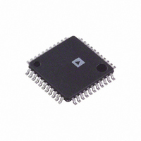
AD6640ASTZ Analog Devices Inc, AD6640ASTZ Datasheet - Page 12

AD6640ASTZ
Manufacturer Part Number
AD6640ASTZ
Description
12-BIT 65 MSPS MONOLITHIC A/D CONVERTER
Manufacturer
Analog Devices Inc
Datasheet
1.AD6640STPCB.pdf
(24 pages)
Specifications of AD6640ASTZ
Function
A/D Converter
Rf Type
Cellular/PCS, GPS
Secondary Attributes
12 Bit, 65MSPS
Package / Case
44-LQFP
Lead Free Status / RoHS Status
Lead free / RoHS Compliant
Available stocks
Company
Part Number
Manufacturer
Quantity
Price
Part Number:
AD6640ASTZ
Manufacturer:
ADI/亚德诺
Quantity:
20 000
AD6640
If a low jitter ECL clock is available, another option is to ac-couple
a differential ECL signal to the ENCODE input pins as shown in
Figure 12. The capacitors shown here should be chip capacitors
but do not need to be of the low inductance variety.
As a final alternative, the ECL gate may be replaced by an ECL
comparator. The input to the comparator could then be a logic
signal or a sine signal.
Driving the Analog Input
Because the AD6640 operates from a single 5 V supply, the
analog input voltage range is offset from ground by 2.4 V. Each
analog input connects through a 450 Ω resistor to the 2.4 V bias
voltage and to the input of a differential buffer (Figure 14). This
resistor network on the input properly biases the followers for
maximum linearity and range. Therefore, the analog source driving
the AD6640 should be ac-coupled to the input pins. Since the
differential input impedance of the AD6640 is 0.9 kΩ, the analog
input power requirement is only –3 dBm, simplifying the drive
amplifier in many cases.
SOURCE
0.1 F
Figure 11. Sine Source–Differential ENCODE
SINE
50
Figure 13. ECL Comparator for ENCODE
Figure 12. Differential ECL for ENCODE
Figure 14. Differential Analog Inputs
GATE
0.01 F
ECL
AD96687 (1/2)
510
V
AIN
AIN
510
REF
–V
S
T1–1T
510
–V
450
450
S
0.1 F
0.1 F
510
BUF
0.1 F
0.1 F
BUF
BUF
R
ENCODE
ENCODE
ENCODE
ENCODE
ENCODE
ENCODE
REFERENCE
AD6640
AD6640
2.4V
AD6640
AD6640
–12–
To take full advantage of this high input impedance, a 20:1 trans-
former would be required. This is a large ratio and could result
in unsatisfactory performance. In this case, a lower step-up
ratio could be used. For example, if R
along with a 4:1 transformer, the input would match to a 50 Ω
source with a full-scale drive of 4 dBm (Figure 15). Note that the
external load resistor, R
input resistance of 900 Ω. The external resistor value can be
calculated from the following equation:
where Z is the desired impedance (200 Ω for a 4:1 transformer
with 50 Ω input source).
If the lower drive power is attractive, a combination transformer
match and LC match could be employed that would use a 4:1
transformer with an LC as shown in Figure 16. This solution is
useful when good performance in the third Nyquist zone is
required. Such a requirement arises when digitizing high inter-
mediate frequencies in communications receivers.
In applications where gain is needed but dc-coupling is not
necessary, an extension of Figure 16 is recommended. A 50 Ω
gain block may be placed in front of the LC matching network.
Such gain blocks are readily available for commercial applications.
These low cost modules can have excellent NF and intermodulation
performance. This circuit is especially good for the “IF” receiver
application previously mentioned.
In applications where dc-coupling is required, the circuit in
Figure 17 can be used. It should be noted that the addition of
circuitry for dc-coupling may compromise performance in terms of
noise, offset, and dynamic performance. This circuit requires an
inverting and noninverting signal path. Additionally, an offset must
be generated so that the analog input to each pin is centered
near 2.4 V. Since the input is differential, small differences in
the dc voltage at each input can translate into an offset for the
circuit. The same holds true for gain mismatch. Therefore, some
means of adjusting the gain and offset between the sides should
Figure 15. Transformer-Coupled Analog Input Signal
ANALOG
SIGNAL
–3dBm
AT
ANALOG
SIGNAL
Figure 16. Low Power Drive Circuit
INPUT
0.1 F
+j100
–j125
T
0.1 F
, is in parallel with the AD6640 analog
R
1:4
0.01 F
T
=
Z
1
0.01 F
–
R
1
1:4
900
T
1
T
AIN
V
AIN
REF
were set to 260 Ω,
AD6640
V
AIN
AIN
REF
AD6640
REV. A


