AD6640ASTZ Analog Devices Inc, AD6640ASTZ Datasheet - Page 13
AD6640ASTZ
Manufacturer Part Number
AD6640ASTZ
Description
12-BIT 65 MSPS MONOLITHIC A/D CONVERTER
Manufacturer
Analog Devices Inc
Datasheet
1.AD6640STPCB.pdf
(24 pages)
Specifications of AD6640ASTZ
Function
A/D Converter
Rf Type
Cellular/PCS, GPS
Secondary Attributes
12 Bit, 65MSPS
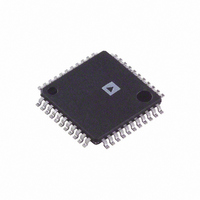
Package / Case
44-LQFP
Lead Free Status / RoHS Status
Lead free / RoHS Compliant
Available stocks
Company
Part Number
Manufacturer
Quantity
Price

Part Number:
AD6640ASTZ
Manufacturer:
ADI/亚德诺
Quantity:
20 000


REV. A
be implemented. The addition of small value resistors between the
AD9631 and the AD6640 will prevent oscillation due to the
capacitive input of the ADC.
Power Supplies
Care should be taken when selecting a power source. Linear
supplies are strongly recommended as switching supplies tend to
have radiated components that may be “received” by the
AD6640. Each of the power supply pins should be decoupled as
closely to the package as possible using 0.1 µF chip capacitors.
The AD6640 has separate digital and analog 5 V pins. The analog
supplies are labeled AV
DV
best performance is achieved when the supplies are separate. This
is because the fast digital output swings can couple switching
noise back into the analog supplies. Note that AV
within 5% of 5 V; however, the DV
ing to output digital logic family (i.e., DV
to the same supply as the digital circuitry). The AD6640 is specified
for DV
Output Loading
Care must be taken when designing the data receivers for the
AD6640. It is recommended that the digital outputs drive a series
resistor (e.g., 348 Ω) followed by a gate like the 74LCX574.
To minimize capacitive loading, there should only be one gate on
each output pin. An example of this is shown in the evaluation
board schematic shown in Figure 18. The digital outputs of the
AD6640 have a constant rise time output stage. The output
slew rate is about 1 V/ns when DV
gate combined with PCB trace and through hole will have a load
of approximately 10 pF. Therefore, as each bit switches:
10 mA
out of the device. A full-scale transition can cause up to 120 mA
(12 bits
stages. The series resistor will minimize the output currents that
can flow in the output stage. These switching currents are con-
fined between ground and the DV
should be avoided since they can appreciably add to the dynamic
switching currents of the AD6640.
SOURCE
SIGNAL
CC
. Although analog and digital supplies may be tied together,
CC
10 pF ×
Figure 17. DC-Coupled Analog Input Circuit
= 3.3 V as this is a common supply for digital ASICs.
10 mA/bit) of current to flow through the digital output
350
62
78
0.1 F
1ns
1V
OP279
(1/2)
1000
of dynamic current per bit will flow in or
467
467
CC
and the digital supply pins are labeled
127
425
750
OP279
CC
(1/2)
CC
AD9631
AD9631
350
CC
350
supply may be varied accord-
pin. Standard TTL gates
= 5 V. A typical CMOS
0.1 F
CC
15
should be connected
15
0.01 F
CC
must be held
AIN
AIN
V
AD6640
REF
–13–
Layout Information
The schematic of the evaluation board (Figure 18) represents
a typical implementation of the AD6640. The pinout of the
AD6640 facilitates ease of use and the implementation of high
frequency/high resolution design practices. All of the digital
outputs are on one side while the other sides contain all of the
inputs. It is highly recommended that high quality ceramic chip
capacitors be used to decouple each supply pin to ground directly
at the device. Depending on the configuration used for the
ENCODE and analog inputs, one or more capacitors are required
on those input pins. The capacitors used on the ENCODE and
V
previously in this data sheet.
A multilayer board is recommended to achieve best results. Care
should be taken when placing the digital output runs. Because the
digital outputs have such a high slew rate, the capacitive loading
on the digital outputs should be minimized. Circuit traces for
the digital outputs should be kept short and connect directly to
the receiving gate (broken only by the insertion of the series
resistor). Digital data lines should be kept clear of analog and
ENCODE traces.
Evaluation Boards
The evaluation board for the AD6640 is very straightforward,
consisting of power, signal inputs, and digital outputs. The
evaluation board includes the option for an onboard clock oscil-
lator for the ENCODE.
Power to the analog supply pins is connected via banana jacks.
The analog supply powers the crystal oscillator and the AV
pins of the AD6640.
The DV
digital supply connection also powers the digital gates on the PCB.
By maintaining separate analog and digital power supplies, degra-
dation in SNR and SFDR is kept to a minimum. Total power
requirement is approximately 200 mA. This configuration allows
for easy evaluation of different logic families (i.e., connection
to a 3.3 V logic board).
The analog input is connected via J2 and is transformer-coupled
to the AD6640 (see Driving the Analog Input section). The
onboard termination resistor is 270 Ω. This resistor, in parallel
with the AD6640’s input resistance (900 Ω), provides a 50 Ω load
to the analog source driving the 1:4 transformer. If a different
input impedance is required, replace R16 by using the equation
where Z is desired input impedance (200 Ω for a 4:1 transformer
with 50 Ω source).
The analog input range of the PCB is ±0.5 V (i.e., signal ac-coupled
to AD6640).
The ENCODE signal may be generated using an onboard crystal
oscillator, U1. The oscillator is socketed and may be replaced by
an external ENCODE source via J1. If an external source is used,
it should be a high quality TTL source. A transformer converts
the single-ended TTL signal to a differential clock (see Encoding
the AD6640 section). Since the ENCODE is coupled with a
transformer, a sine wave could have been used; note, however,
that U5 requires TTL levels to function properly.
REF
pins must be a low inductance chip capacitor as referenced
CC
power is supplied via J3, the digital interface. This
R16 =
Z
1
−
1
900
1
AD6640
CC
Related parts for AD6640ASTZ
Image
Part Number
Description
Manufacturer
Datasheet
Request
R

Part Number:
Description:
±1.7g Dual-Axis IMEMS Accelerometer Evaluation Board
Manufacturer:
Analog Devices Inc
Datasheet:

Part Number:
Description:
Inertial Sensor Evaluation System
Manufacturer:
Analog Devices Inc
Datasheet:
Part Number:
Description:
Manufacturer:
Analog Devices Inc
Datasheet:
Part Number:
Description:
Manufacturer:
Analog Devices Inc
Datasheet:
Part Number:
Description:
Manufacturer:
Analog Devices Inc
Datasheet:
Part Number:
Description:
Manufacturer:
Analog Devices Inc
Datasheet:
Part Number:
Description:
Manufacturer:
Analog Devices Inc
Datasheet:
Part Number:
Description:
Manufacturer:
Analog Devices Inc
Datasheet:
Part Number:
Description:
Manufacturer:
Analog Devices Inc
Datasheet:
Part Number:
Description:
Manufacturer:
Analog Devices Inc
Datasheet:
Part Number:
Description:
Manufacturer:
Analog Devices Inc
Datasheet:
Part Number:
Description:
Manufacturer:
Analog Devices Inc
Datasheet:
Part Number:
Description:
Manufacturer:
Analog Devices Inc
Datasheet: