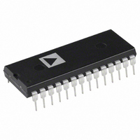
AD664JN-BIP Analog Devices Inc, AD664JN-BIP Datasheet - Page 8

AD664JN-BIP
Manufacturer Part Number
AD664JN-BIP
Description
D/A Converter (D-A) IC
Manufacturer
Analog Devices Inc
Datasheet
1.AD664JNZ-BIP.pdf
(20 pages)
Specifications of AD664JN-BIP
Supply Voltage
15V
No. Of Bits
12 Bit
Mounting Type
Through Hole
Interface Type
Parallel
Package / Case
28-DIP
Rohs Status
RoHS non-compliant
Settling Time
8µs
Number Of Bits
12
Data Interface
Parallel
Number Of Converters
4
Voltage Supply Source
Dual ±
Power Dissipation (max)
525mW
Operating Temperature
0°C ~ 70°C
Number Of Channels
4
Resolution
12b
Conversion Rate
125KSPS
Single Supply Voltage (typ)
Not RequiredV
Dual Supply Voltage (typ)
±15V
Architecture
R-2R
Power Supply Requirement
Dual
Output Type
Voltage
Single Supply Voltage (min)
Not RequiredV
Single Supply Voltage (max)
Not RequiredV
Dual Supply Voltage (min)
±11.4V
Dual Supply Voltage (max)
±16.5V
Operating Temp Range
0C to 70C
Operating Temperature Classification
Commercial
Mounting
Through Hole
Pin Count
28
Lead Free Status / Rohs Status
Not Compliant
Available stocks
Company
Part Number
Manufacturer
Quantity
Price
AD664
The following sections detail the timing requirements for
various data loading schemes. All of the timing specifica-
tions shown assume V
V
Load and Update One DAC Output
In this first example, the object is simply to change the output of
one of the four DACs on the AD664 chip. The procedure is to
select the address bits that indicate the DAC to be programmed,
pull LATCH SELECT (LS) low, pull CHIP SELECT (CS)
low, release LS and then release CS. When CS goes low, data
enters the first rank of the input latch. As soon as LS goes high,
the data is transferred into the second rank and produces the
new output voltage. During this transfer, MS, TR, RD and RST
should be held high.
Preloading the First Rank of One DAC
In this case, the object is to load new data into the first rank of
one of the DACs but not the output. As in the previous case, the
address and data inputs are placed on the appropriate pins. LS
is then brought to “0” and then CS is asserted. Note that in this
situation, however, CS goes high before LS goes high. The in-
put data is prevented from getting to the second rank and affect-
ing the output voltage.
EE
= –15 V and V
Function
Load 1st Rank (data)
Load 2nd Rank (data)
Readback 2nd Rank (data)
Reset
Transparent
Mode Select
Readback Mode
Update 2nd Rank
NOTES
X = Don’t Care.
1
2
For 44-pin versions only. Allow the AD664 to be addressed in 4-bit nibble, 8-bit byte or 12-bit parallel words.
For MS, TR, LS = 0, a MS 1st write occurs.
DACA
DACB
DACC
DACD
All DACs
1st Rank
2nd Rank
and Mode
DACA
DACB
DACC
DACD
LL
1
1, 2
= +5 V.
1
IH
= 2.4 V, V
IL
DS1, DS0
00
01
10
11
XX
Select D/A
XX
XX
00
01
10
11
XX
XX
XX
XX
= 0.4 V, V
Table II. AD664 Digital Truth Table
CC
= +15 V,
LS
0
0
0
0
1
X
X
1
0
0
0
0
0
1
X
1
MS
1
1
1
1
1
1
1
1
1
0
1
1
X
0
0
0
–8–
TR
1
1
1
1
1
1
X
0
0
0
0
0
1
1
1
0
Figure 9b. Update Output of a Single DAC Timing
Figure 9a. Update Output of a Single DAC
QS0, 1, 2
Select Quad
Select Quad
Select Quad
Select Quad
XXX
Select Quad
XXX
000
000
000
000
000
00X
XXX
00X
XXX
SYMBOL
t
t
t
t
t
t
t
*FOR t
LS
DS
DH
LW
CH
AS
AH
INCREASED BY THE SAME AMOUNT THAT
t
LS
*
IS GREATER THAN 0 ns.
LS
> 0, THE WIDTH OF LS MUST BE
1
25 C
MIN (ns)
0
0
0
60
30
0
0
RD
1
1
1
1
1
0
X
1
1
1
1
1
1
1
0
1
T
MIN (ns)
0
0
0
80
50
0
0
MIN
1 0
1 0
1 0
1 0
1 0
CS
1 0
1 0
X
1 0
1 0
1 0
1 0
1 0
1 0
1 0
1 0
to T
MAX
RST
1
1
1
1
1
1
0
1
1
1
1
1
1
1
1
1
REV. C


