AD760AQ Analog Devices Inc, AD760AQ Datasheet
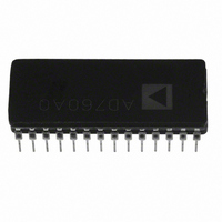
Digital-Analog Converter IC

AD760AQ

Manufacturer Part Number
AD760AQ
Description
Digital-Analog Converter IC
Manufacturer
Analog Devices Inc
Series
DACPORT®r
Datasheet

Specifications of AD760AQ

Rohs Status
RoHS non-compliant
Settling Time
6µs
Number Of Bits
16
Data Interface
Serial, Parallel
Number Of Converters
1
Voltage Supply Source
Dual ±
Power Dissipation (max)
725mW
Operating Temperature
-40°C ~ 85°C
Mounting Type
Through Hole
Package / Case
28-CDIP (0.600", 15.24mm)
Lead Free Status / RoHS Status

Available stocks

Company
Part Number
Manufacturer
Quantity
Price
Part Number:
AD760AQZ
Manufacturer:
INTEL
Quantity:
32
a
PRODUCT DESCRIPTION
The AD760 is a complete 16/18-bit self-calibrating monolithic
DAC (DACPORT®) with onboard voltage reference, double
buffered latches and output amplifier. It is manufactured on
Analog Devices’ BiMOS II process. This process allows the fab-
rication of low power CMOS logic functions on the same chip
as high precision bipolar linear circuitry.
Self-calibration is initiated by simply pulsing the CAL pin low.
The CALOK pin indicates when calibration has been success-
fully completed. The output multiplexer (MUX
to send the output to the bottom of the output range during
calibration.
Data can be loaded into the AD760 as straight binary, serial
data or as two 8-bit bytes. In serial mode, 16-bit or 18-bit data
can be used and the serial mode input format is pin selectable,
to be MSB or LSB first. This is made possible by three digital
input pins which have dual functions (Pins 12, 13, and 14). In
byte mode the user can similarly define whether the high byte or
low byte is loaded first. The serial output (S
user to daisy chain several AD760s by shifting the data through
the input latch into the next DAC thus minimizing the number
of control lines required in a multiple DAC application. The
double buffered latch structure eliminates data skew errors and
provides for simultaneous updating of DACs in a multi-DAC
system.
The asynchronous CLR function can be configured to clear the
output to minus full-scale or midscale depending on the state of
Pin 17 when CLR is strobed. The AD760 also powers up with the
REV. A
Information furnished by Analog Devices is believed to be accurate and
reliable. However, no responsibility is assumed by Analog Devices for its
use, nor for any infringements of patents or other rights of third parties
which may result from its use. No license is granted by implication or
otherwise under any patent or patent rights of Analog Devices.
FEATURES
±0.2 LSB (±0.00031%) Typ Peak DNL and INL
±0.5 LSB (±0.00076%) Typ Unipolar Offset, Bipolar Zero
17-Bit Monotonicity Guaranteed
18-Bit Resolution (in Serial Mode)
Complete 16/18-Bit D/A Function
Microprocessor Compatible
Asynchronous Clear Function
Serial Output Pin Facilitates Daisy Chaining
Pin Strappable Unipolar or Bipolar Output
Low THD+N: 0.005%
MUX Output Control on Power-Up and Supply Glitches
On-Chip Output Amplifier
On-Chip Buried Zener Voltage Reference
Serial or Byte Input
Double Buffered Latches
OUT
OUT
) pin allows the
) can be used
MUX output in a predetermined state by means of a digital and
analog power supply detection circuit. This is particularly use-
ful for robotic and industrial control applications.
The AD760 is available in a 28-pin, 600 mil cerdip package.
The AQ version is specified from –40°C to +85°C.
DACPORT is a registered trademark of Analog Devices, Inc.
One Technology Way, P.O. Box 9106, Norwood. MA 02062-9106, U.S.A.
Tel: 617/329-4700
REF OUT
BIP CLR
OR LBE
REF IN
LDAC
HBE
SER
CLR
UNI/
–0.25
–0.75
0.75
0.25
17
18
19
20
21
25
26
0
0
16/18-Bit Self-Calibrating
FUNCTIONAL BLOCK DIAGRAM
+10V
V
R
C
REF
Typical Integral Nonlinearity
CALOK
OUT
L
L
CS
16
= 2k
= 1000pF
1
9.95k
= –10V TO +10V
S
OR
DB0
16384
14
IN
Serial/Byte DACPORT
CAL
16/18-BIT DAC LATCH
CALIBRATION SEQUENCER
2
CALIBRATION DAC
INPUT REGISTER
MSB/
LSB
OR
DB1
INPUT CODE – Decimal
13
16/18-BIT
MAIN DAC
–V
RAM
DB2
18/16
SERIAL
OR
12
3
EE
32768
+V
4
CC
DB7
© Analog Devices, Inc., 1995
7
+V
49152
5
LL
AD760
AD760
10k
10k
DGND
Fax: 617/326-8703
6
65535
15
24
23
27
28
22
S
SPAN/
BIP
OFF
V
MUX
MUX
AGND
OUT
OUT
OUT
I N

Related parts for AD760AQ

AD760AQ Summary of contents

Page 1

FEATURES ±0.2 LSB (±0.00031%) Typ Peak DNL and INL ±0.5 LSB (±0.00076%) Typ Unipolar Offset, Bipolar Zero 17-Bit Monotonicity Guaranteed 18-Bit Resolution (in Serial Mode) Complete 16/18-Bit D/A Function On-Chip Output Amplifier On-Chip Buried Zener Voltage Reference Microprocessor Compatible ...

Page 2

... Current (No Load 5 2 Power Supply Sensitivity with OUT Power Dissipation (Static, No Load) TEMPERATURE RANGE Specified Performance ( +25° + AD760AQ Min 16/18 2 +85° 9. –10 5 0.9 2.0 0 2.4 +14.25 –15.75 +4.75 –21 –40 –2– = – unless otherwise noted) LL Typ Max Units Bits ± ...

Page 3

NOTES 1 For 18-bit resolution, 1 LSB = 0.00038% of FSR. For 16-bit resolution, 1 LSB = 0.0015% of FSR. For 14-bit resolution, 1 LSB = 0.006% of FSR. FSR stands for full-scale range and unipolar ...

Page 4

AD760 TIMING CHARACTERISTICS Limit Parameter +25°C T MIN (Figure 1a BES BEH t 200 350 (Figure 1b) ...

Page 5

... Exposure to absolute maximum rating conditions for extended periods may affect device reliability. Model AD760AQ CAUTION ESD (electrostatic discharge) sensitive device. Electrostatic charges as high as 4000 V readily accumulate on the human body and test equipment and can discharge without detection. ...

Page 6

AD760 DEFINITIONS OF SPECIFICATIONS INTEGRAL NONLINEARITY: Analog Devices defines inte- gral nonlinearity as the maximum deviation of the actual, ad- justed DAC output from the ideal analog output (a straight line drawn from – 1 LSB) for ...

Page 7

CALIBRATED LINEARITY PERFORMANCE The cumulative probability plots for the AD760 INL and DNL shown in Figures 3 and 4 represent the maximum absolute- value (peak) linearity error for each part. Roughly 100 parts from each of 3 wafer lots were ...

Page 8

AD760 AD760 REFIN 25 REFOUT +10V REF 26 9.95k 10k 24 SPAN/ 10k BIP OFF MAIN DAC 23 V Figure 6a ±10 V Bipolar Voltage Output Gain Error can be adjusted to zero using the circuit shown ...

Page 9

The digital-to-analog glitch impulse is specified as 15 nV-s typi- cal. Figure 8c shows the typical glitch impulse characteristic at the code 011 . . . 111 to 100 . . . 000 transition when loading the second rank register ...

Page 10

AD760 Byte Mode Operation is enabled by setting SER high, which configures DB0–DB7 as data inputs. In this mode HBE and LBE are used to identify the data as either the high byte or the low byte of the 16-bit ...

Page 11

The HC11 generates the requisite 8 clock pulses with data valid on the rising edges. After the most significant byte is transmit- ted, the least significant byte (LSBY) is loaded from memory and transmitted in a similar fashion. To complete ...

Page 12

AD760 One feature that the AD760 incorporates to help the user layout is that the analog pins ( REF OUT, REF IN, SPAN BIP OFFSET MUX , MUX OUT OUT IN cent to ...

Related keywords