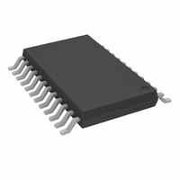
AD8186ARUZ Analog Devices Inc, AD8186ARUZ Datasheet - Page 16

AD8186ARUZ
Manufacturer Part Number
AD8186ARUZ
Description
IC,ANALOG MUX,TRIPLE,2-CHANNEL,BIPOLAR,TSSOP,24PIN,PLASTIC
Manufacturer
Analog Devices Inc
Type
Analog Multiplexerr
Datasheet
1.AD8186ARUZ.pdf
(20 pages)
Specifications of AD8186ARUZ
Rohs Compliant
YES
Function
Multiplexer
Circuit
3 x 2:1
On-state Resistance
350 mOhm
Voltage Supply Source
Single Supply
Voltage - Supply, Single/dual (±)
3.5 V ~ 5.5 V
Current - Supply
15mA
Operating Temperature
-40°C ~ 85°C
Mounting Type
Surface Mount
Package / Case
24-TSSOP (0.173", 4.40mm Width)
Package
24TSSOP
Multiplexer Architecture
2:1
Maximum Turn-off Time
17(Typ)@5V ns
Maximum Turn-on Time
4(Typ)@5V ns
Power Supply Type
Single
Lead Free Status / RoHS Status
Lead free / RoHS Compliant
Available stocks
Company
Part Number
Manufacturer
Quantity
Price
Part Number:
AD8186ARUZ
Manufacturer:
ADI/亚德诺
Quantity:
20 000
Part Number:
AD8186ARUZ-R7
Manufacturer:
ADI/亚德诺
Quantity:
20 000
Part Number:
AD8186ARUZ-RL
Manufacturer:
ADI/亚德诺
Quantity:
20 000
AD8186/AD8187
A dc restore circuit using the AD8187 is shown in Figure 11.
Two separate sources of RGB video are ac-coupled to the
0.1 µF input capacitors of the AD8187. The input points of
the AD8187 are switched to a 1.5 V reference by the ADG786,
which works in the following manner:
The SEL A/B signal selects the A or B inputs to the AD8187. It
also selects the switch positions in the ADG786 such that the
same selected inputs will be connected to V
During the horizontal interval, all of the RGB input signals are at
a flat black level. A logic signal that is low during HSYNC is
applied to the EN of the ADG786. This closes the switches
and clamps the black level to 1.5 V. At all other times, the switches
are off and the node at the inputs to the AD8187 floats.
There are two considerations for sizing the input coupling capaci-
tors. One is the time constant during the H-pulse clamping. The
other is the droop associated with the capacitor discharge due to the
input bias current of the AD8187. For the former, it is better to
have a small capacitor; but for the latter, a larger capacitor is better.
The ON resistance of the ADG786 and the coupling capacitor
forms the time constant of the input clamp. The ADG786 ON
resistance is 5 Ω max. With a 0.1 µF capacitor, a time constant
of 0.5 µs is created. Thus, a sync pulse of greater than 2.5 µs will
cause less than 1% error. This is not critical because the black
level from successive lines is very close and the voltage changes
little from line to line.
A rough approximation for the horizontal line time for a graphics
system is 30 µs. This will vary depending on the resolution and
the vertical rate. The coupling capacitor needs to hold the voltage
relatively constant during this time while the input bias current
of the AD8187 is discharging it.
2.4V MIN
0.8V MIN
3.48k
1.5k
5V
10 F
1.5V
HSYNC
+
SEL A/B
V
Figure 11. AD8187 AC-Coupled with DC Restore
REF
0.1 F
REF
when EN is low.
D1
D2
D3
GND
EN A0 A1 A2
ADG786
LOGIC
V
5V
DD
S1A
S1B
S2A
S2B
S3A
S3B
V
SS
–16–
GRNA
GRNB
REDA
REDB
BLUA
BLUB
The change in voltage is I
the capacitance. With an I
and a 0.1 µF coupling capacitor, the amount of droop is
0.75 mV. This is roughly 0.1% of the full video amplitude and
will not be observable in the video display.
High Speed Design Considerations
The AD8186/AD8187 are extremely high speed switching ampli-
fiers for routing the highest resolution graphic signals. Extra care
is required in the circuit design and layout to ensure that the full
resolution of the video is realized.
First, the board should have at least one layer of a solid ground
plane. Long signal paths should be referenced to a ground plane
as controlled-impedance traces. All bypass capacitors should be
very close to the pins of the part with absolutely minimum extra
circuit length in the path. It is also helpful to have a large V
plane on a circuit board layer that is closely spaced to the ground
plane. This creates a low inductance interplane capacitance,
which is very helpful in supplying the fast transient currents that
the part demands during high resolution signal transitions.
Evaluation Board
An evaluation board has been designed and is offered for run-
ning the AD8186/AD8187 on a single supply. The inputs and
outputs are ac-coupled and terminated with 75 Ω resistors.
For the AD8187, a potentiometer is provided to allow setting
V
The logic control signals can be statically set by adding or
removing a jumper. If it is required to drive the logic pins
with a fast signal, an SMA connector can be used to deliver the
signal, and a place for a termination resistor is provided.
REF
0.1 F
0.1 F
0.1 F
0.1 F
0.1 F
0.1 F
V
REF
at any value between V
IN0A
IN1A
IN2A
V
IN0B
IN1B
IN2B
D
REF
GND
3V TO 5V
DV
V
EE
CC
V
SEL A/B
5V
CC
AD8187
2
2
2
BIAS
BIAS
CC
OUT0
OUT1
OUT2
times the line time divided by
OE
and ground.
of 2.5 µA, a line time of 30 µs,
RED
GRN
BLU
REV. A
CC


