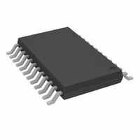
AD8186ARUZ-R7 Analog Devices Inc, AD8186ARUZ-R7 Datasheet

AD8186ARUZ-R7
Specifications of AD8186ARUZ-R7
Available stocks
Related parts for AD8186ARUZ-R7
AD8186ARUZ-R7 Summary of contents
Page 1
FEATURES Fully Buffered Inputs and Outputs Fast Channel-to-Channel Switching Single-Supply Operation (5 V) High Speed: 480 MHz Bandwidth (–3 dB p-p >1600 +1) >1500 +2) Fast Settling ...
Page 2
AD8186/AD8187–SPECIFICATIONS Parameter DYNAMIC PERFORMANCE –3 dB Bandwidth (Small Signal) –3 dB Bandwidth (Large Signal) 0.1 dB Flatness Slew Rate (10% to 90% Rise Time) Settling Time to 0.1% NOISE/DISTORTION PERFORMANCE Differential Gain Differential Phase All Hostile Crosstalk Channel-to-Channel Crosstalk, RTI ...
Page 3
Parameter SWITCHING CHARACTERISTICS Channel-to-Channel Switching Time ENABLE to Channel ON Time DISABLE to Channel OFF Time Channel Switching Transient (Glitch) Output Enable Transient (Glitch) DIGITAL INPUTS Logic 1 Voltage Logic 0 Voltage Logic 1 Input Current Logic 0 Input Current ...
Page 4
AD8186/AD8187 ABSOLUTE MAXIMUM RATINGS Supply Voltage . . . . . . . . . . . . . . . . . . . . . . . . . . . . . . . . . 5.5 ...
Page 5
DUT 2 50 52.3 1 GAIN 0 –1 –2 FLATNESS –3 –4 –5 –6 0.1 1.0 10.0 100.0 FREQUENCY (MHz) TPC 1. AD8186 Frequency Response Ω 200 mV p-p, R OUT L 1 ...
Page 6
AD8186/AD8187 0 –10 –20 –30 –40 –50 –60 –70 –80 –90 –100 –110 0 FREQUENCY (MHz) TPC 7. AD8186 All Hostile Crosstalk* vs. Frequency 0 –10 –20 –30 –40 –50 –60 –70 –80 –90 –100 –110 0.1 1.0 ...
Page 7
THIRD –70 –80 –90 –100 10 1 FREQUENCY (MHz) TPC 13. AD8186 Harmonic Distortion vs. Frequency = 150 Ω p-p, R OUT L 0 –10 –20 –30 –40 –PSRR ...
Page 8
AD8186/AD8187 10000 1000 100 10 1 0.1 0 FREQUENCY (MHz) TPC 19. AD8186 Input Impedance vs. Frequency 1000 100 10 1 0.1 0 FREQUENCY (MHz) TPC 20. AD8186 Enabled Output Impedance vs. Frequency 10000 1000 100 ...
Page 9
INPUT 2.60 2.50 2.40 2.30 2.20 OUTPUT 2.10 2.00 1.90 1. TIME (ns) TPC 25. AD8186 Small Signal Pulse Response Ω 200 mV p-p, R OUT L 3.0 2.5 ...
Page 10
AD8186/AD8187 t SETTLED t 0 TIME (2ns/DIV) TPC 31. AD8186 Settling Time (0.1%), = 1 k Ω Step, R OUT L 2.3 1.8 SEL A/B 1.3 0.8 0.3 –0.3 OUTPUT –0.8 –1.3 –1.8 –2.3 –2.8 0 ...
Page 11
OE 1.5 1.0 0.5 0 OUTPUT –0.5 –1.0 –1 120 TIME (ns) TPC 37. AD8186 Enable ON/OFF Time OUT 1.5 OE 1.0 0.5 OUTPUT ...
Page 12
AD8186/AD8187 THEORY OF OPERATION The AD8186 (G = +1) and AD8187 (G = +2) are single-supply, triple 2:1 multiplexers with TTL compatible global input switch- ing and output-enable control. Optimized for selecting between two RGB (red, green, blue) video sources, ...
Page 13
The AD8187 The AD8187 uses on-chip feedback resistors to realize the gain- of-two function. To provide low crosstalk and a high output impedance when disabled, each set of 500 Ω feedback resistors is terminated by a dedicated reference buffer. A ...
Page 14
AD8186/AD8187 AC-Coupled Inputs (DC Restore before Mux Input) Using ac-coupled inputs presents an interesting challenge for video systems operating from a single 5 V supply. In NTSC and PAL video systems, 700 mV is the approximate difference between the maximum ...
Page 15
APPLICATION Single-Supply Operation The AD8186/AD8187 are targeted mainly for use in single- supply 5 V systems. For operating on these supplies, both V and D should be tied to ground. The control logic pins will GND be referenced to ground. ...
Page 16
AD8186/AD8187 A dc restore circuit using the AD8187 is shown in Figure 11. Two separate sources of RGB video are ac-coupled to the 0.1 µF input capacitors of the AD8187. The input points of the AD8187 are switched to a ...
Page 17
EVALUATION BOARD REV. A Figure 12. Component Side Board Layout Figure 13. Circuit Side Board Layout –17– AD8186/AD8187 ...
Page 18
AD8186/AD8187 Figure 14. Component Side Silkscreen Figure 15. Circuit Side Silkscreen –18– REV. A ...
Page 19
REV. A Figure 16. Single-Supply Evaluation Board –19– AD8186/AD8187 ...
Page 20
AD8186/AD8187 24-Lead Thin Shrink Small Outline Package [TSSOP] PIN 1 0.15 0.05 Revision History Location 6/03—Data Sheet changed from REV REV. A. Changes to SPECIFICATIONS . . . . . . . . . . . . . ...


