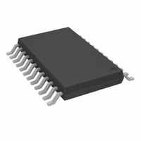
AD8188ARUZ Analog Devices Inc, AD8188ARUZ Datasheet

AD8188ARUZ
Specifications of AD8188ARUZ
Available stocks
Related parts for AD8188ARUZ
AD8188ARUZ Summary of contents
Page 1
FEATURES Fully buffered inputs and outputs Fast channel-to-channel switching Single-supply operation (5 V) High speed 350 MHz bandwidth (−3 dB) @ 200 mV p-p 300 MHz bandwidth (−3 dB p-p Slew rate: 1000 V/μs Fast ...
Page 2
AD8188/AD8189 TABLE OF CONTENTS Features .............................................................................................. 1 Applications....................................................................................... 1 Functional Block Diagram .............................................................. 1 General Description ......................................................................... 1 Revision History ............................................................................... 2 Specifications..................................................................................... 3 Absolute Maximum Ratings............................................................ 5 Thermal Resistance ...................................................................... 5 Maximum Power Dissipation ..................................................... 5 ESD Caution.................................................................................. 5 ...
Page 3
SPECIFICATIONS T = 25°C. For the AD8188 Table 1. Parameter DYNAMIC PERFORMANCE −3 dB Bandwidth (Small Signal) −3 dB Bandwidth (Large Signal) 0.1 dB Flatness Slew Rate (10% to 90% Rise Time) ...
Page 4
AD8188/AD8189 Parameter Disable-to-Channel Off Time Channel Switching Transient (Glitch) Output Enable Transient (Glitch) DIGITAL INPUTS Logic 1 Voltage Logic 0 Voltage Logic 1 Input Current Logic 0 Input Current Conditions 50% logic to 50% output settling, input = 1 V ...
Page 5
ABSOLUTE MAXIMUM RATINGS Table 2. 1 Parameter Supply Voltage GND GND IN0A, IN0B, IN1A, IN1B, IN2A, IN2B, V REF SEL A/B, OE Output Short-Circuit Operation Operating Temperature ...
Page 6
AD8188/AD8189 PIN CONFIGURATION AND FUNCTION DESCRIPTIONS Table 4. Pin Function Descriptions Pin No. Mnemonic Description 1 IN0A Input, High Ground Reference for Digital Control Circuitry. GND 3 IN1A Input, High AD8188: Bypass point for internal reference. ...
Page 7
TYPICAL PERFORMANCE CHARACTERISTICS 3 976Ω DUT 2 50Ω 52.3Ω 1 GAIN 0 –1 –2 FLATNESS –3 –4 –5 –6 0 100 FREQUENCY (MHz) Figure 5. AD8188 Frequency Response, V OUT 1 0 –1 –2 –3 –4 –5 150Ω ...
Page 8
AD8188/AD8189 0 –10 –20 –30 –40 –50 –60 –70 –80 –90 –100 –110 0 FREQUENCY (MHz) Figure 11. AD8188 All Hostile Crosstalk vs. Frequency (Drive All INxA, Listen to Output with INxB Selected) 0 –10 –20 –30 –40 ...
Page 9
THIRD –70 SECOND –80 –90 –100 1 10 FREQUENCY (MHz) Figure 17. AD8188 THD vs. Frequency p-p, R OUT 0 –10 –20 –30 –PSRR –40 –50 –60 +PSRR –70 ...
Page 10
AD8188/AD8189 10k 1k 100 10 1 0.1 0 FREQUENCY (MHz) Figure 23. AD8188 Input Impedance vs. Frequency 1k 100 10 1 0.1 0 FREQUENCY (MHz) Figure 24. AD8188 Enabled Output Impedance vs. Frequency 10k 1k 100 ...
Page 11
INPUT 2.6 2.5 2.4 2.3 2.2 OUTPUT 2.1 2.0 1.9 1 TIME (ns) Figure 29. AD8188 Small Signal Pulse Response 200 mV p- kΩ OUT L 3.0 INPUT 2.5 ...
Page 12
AD8188/AD8189 t SETTLED t TIME (2ns/DIV) 0 Figure 35. AD8188 Settling Time (0.1%), V 2.3 1.8 SEL A/B 1.3 0.8 0.3 –0.3 OUTPUT –0.8 –1.3 –1.8 –2.3 –2 TIME (ns) Figure 36. AD8188 Channel-to-Channel Switching Time, ...
Page 13
OE 1.5 1.0 0.5 OUTPUT 0 –0.5 –1.0 –1 100 120 140 TIME (ns) Figure 41. AD8188 Enable On/Off Time, V 1.5 OE 1.0 0.5 OUTPUT ...
Page 14
AD8188/AD8189 THEORY OF OPERATION The AD8188 ( and AD8189 ( are single-supply, triple 2:1 multiplexers with TTL-compatible global input switching and output-enable control. Optimized for selecting between two RGB (red, green, blue) video sources, the devices ...
Page 15
AD8188 MUX SYSTEM IN0A IN0B IN1A IN1B IN2A IN2B “C_BYPASS” V REF INTERNAL CAP BIAS REFERENCE DIRECT CONNECTION TO ANY “QUIET” AC GROUND (FOR EXAMPLE, GND AND Figure 45. V Pin Connection for AD8188 ...
Page 16
AD8188/AD8189 5V 10kΩ V 1µF 10kΩ CAP MUST BE LARGE ENOUGH TO ABSORB TRANSIENT CURRENTS WITH MINIMUM BOUNCE. Figure 49. Alternate Method for Synthesis of a False Ground Reference AC-COUPLED INPUTS Using ac-coupled inputs presents an interesting challenge for video ...
Page 17
APPLICATIONS SINGLE-SUPPLY OPERATION The AD8188/AD8189 are targeted mainly for use in single- supply 5 V systems. For operating on these supplies, both V and D should be tied to ground, and the control logic pins GND should be referenced to ...
Page 18
AD8188/AD8189 RGB SOURCE RGB SOURCE RGB SOURCE RGB SOURCE 100Ω 100Ω The circuit in Figure 55 can increase the crosstalk between inputs, because ...
Page 19
These two techniques can also be combined. Typically, crosstalk between the RGB signals from the same source is less objectionable than crosstalk between two different sources. The former can cause a color or luminance shift, but spatially, everything is coherent. ...
Page 20
AD8188/AD8189 HIGH SPEED DESIGN CONSIDERATIONS The AD8188/AD8189 are extremely high speed switching amplifiers for routing the highest resolution graphic signals. Extra care is required in the circuit design and layout to ensure that the full resolution of the video is ...
Page 21
EVALUATION BOARD An evaluation board has been designed and is offered for running the AD8188/AD8189 on a single supply. The inputs and outputs are ac-coupled and terminated with 75 Ω resistors. For the AD8189, a potentiometer is provided to allow ...
Page 22
AD8188/AD8189 Figure 59. Component Side Silkscreen Figure 60. Circuit Side Silkscreen Rev Page ...
Page 23
SCHEMATICS Figure 61. Single-Supply Evaluation Board Rev Page AD8188/AD8189 06239-061 ...
Page 24
... AD8188/AD8189 OUTLINE DIMENSIONS 0.15 0.05 ORDERING GUIDE Model Temperature Range 1 AD8188ARUZ –40°C to +85°C 1 AD8188ARUZ-RL –40°C to +85°C 1 AD8188ARUZ-R7 –40°C to +85°C 1 AD8189ARUZ –40°C to +85°C 1 AD8189ARUZ-RL –40°C to +85°C 1 AD8189ARUZ-R7 –40°C to +85°C 1 AD8188Z-EVALZ 1 ...


