AD845SQ Analog Devices Inc, AD845SQ Datasheet - Page 2
AD845SQ
Manufacturer Part Number
AD845SQ
Description
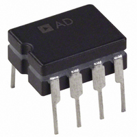
IC,Operational Amplifier,SINGLE,BIPOLAR/JFET,DIP,8PIN,CERAMIC
Manufacturer
Analog Devices Inc
Datasheet
1.AD845JNZ.pdf
(12 pages)
Specifications of AD845SQ
Rohs Status
RoHS non-compliant
Amplifier Type
J-FET
Number Of Circuits
1
Slew Rate
100 V/µs
Gain Bandwidth Product
16MHz
Current - Input Bias
750pA
Voltage - Input Offset
250µV
Current - Supply
10mA
Current - Output / Channel
50mA
Voltage - Supply, Single/dual (±)
±4.75 V ~ 18 V
Operating Temperature
-55°C ~ 125°C
Mounting Type
Through Hole
Package / Case
8-CDIP (0.300", 7.62mm)
Output Type
-
-3db Bandwidth
-
Lead Free Status / RoHS Status
Available stocks
Company
Part Number
Manufacturer
Quantity
Price

Company:
Part Number:
AD845SQ/883
Manufacturer:
Microsemi
Quantity:
1 400
Part Number:
AD845SQ/883B
Manufacturer:
ADI/亚德诺
Quantity:
20 000


AD845–SPECIFICATIONS
Parameter
INPUT OFFSET VOLTAGE
INPUT BIAS CURRENT
INPUT OFFSET CURRENT
INPUT CHARACTERISTICS
INPUT VOLTAGE RANGE
INPUT VOLTAGE NOISE
INPUT CURRENT NOISE
OPEN-LOOP GAIN
OUTPUT CHARACTERISTICS
FREQUENCY RESPONSE
DIFFERENTIAL GAIN
DIFFERENTIAL PHASE
POWER SUPPLY
NOTES
1
2
3
4
All min and max specifications are guaranteed. Specifications shown in boldface are tested on all production units at final electrical test. Results from these tests are
used to calculate outgoing quality levels.
Specifications subject to change without notice.
Input offset voltage specifications are guaranteed after five minutes of operation at T
Bias current specifications are guaranteed maximum at either input after five minutes of operation at T
FPBW = slew rate/2 p V peak.
S grade T
Initial Offset
Offset Drift
Initial
Initial
Input Resistance
Input Capacitance
Differential
Common-Mode
Common-Mode Rejection
Voltage
Current
Output Resistance
Small Signal
Full Power Bandwidth
Rise Time
Overshoot
Slew Rate
Settling Time
Rated Performance
Operating Range
Rejection Ratio
Quiescent Current
MIN
–T
MAX
are tested with automatic test equipment at T
3
2
1
Conditions
T
V
T
V
T
V
0.1 Hz to 10 Hz
f = 10 Hz
f = 100 Hz
f = 1 kHz
f = 10 kHz
f = 100 kHz
f = 1 kHz
V
R
R
T
R
Short Circuit
Open Loop
Unity Gain
V
R
10 V Step
C
R
to 0.01%
to 0.1%
f = 4.4 MHz
f = 4.4 MHz
V
T
MIN
CM
MIN
CM
MIN
CM
O
LOAD
LOAD
MIN
LOAD
O
LOAD
LOAD
S
MIN
LOAD
= ± 5 to ± 15 V 88
= ± 10 V
= ± 10 V
= 0 V
= 0 V
= ± 10 V
–T
to T
to T
to T
to T
≥ 2 kW
≥ 500 W
≥ 500 W
= 500 W
= 500 W
= 100 pF
MAX
MAX
MAX
MAX
MAX
Min
86
200
100
70
12.8
80
10
12.5
4.75
(@ 25 C and
A
= –55∞C and T
AD845J/A
Typ
0.7
0.75
25
10
4.0
± 20
+10.5/–13
110
4
80
60
25
18
12
0.1
500
250
50
5
1.75
20
20
100
350
250
0.04
± 15
110
10
16
0.02
11
–2–
15 V dc, unless otherwise noted.)
A
Max Min
1.5
2.5
20
2
45/75
300
3/6.5
12
A
= +125∞C.
18
= 25∞C.
94
250
125
75
13.6
94
95
10
12.5
4.75
AD845K/B
Typ
0.1
1.5
0.5
15
10
4.0
± 20
+10.5/–13
113
4
80
60
25
18
12
0.1
500
250
50
5
16
1.75
20
20
100
350
250
0.04
0.02
± 15
113
10
A
11
= 25∞C.
Max
0.25
0.4
5.0
1
18/38
100
1.2/2.6
500
12
18
Min
86
200
100
50
13.6
94
88
10
12.5
4.75
AD845S
Typ
0.25
0.75
25
10
4.0
± 20
+10.5/–13
110
4
80
60
25
18
12
0.1
500
250
50
5
16
1.75
20
20
100
350
250
0.04
0.02
± 15
110
10
11
Max
500
1.0
2.0
10
2
300
20
500
12
18
REV. E
Unit
mV
mV
mV/∞C
nA
nA
pA
nA
kW
pF
V
V
dB
mV p-p
nV/÷Hz
nV/÷Hz
nV/÷Hz
nV/÷Hz
nV/÷Hz
pA/÷Hz
V/mV
V/mV
V/mV
V
mA
W
MHz
MHz
ns
%
V/ms
ns
ns
%
Degree
V
V
dB
mA
Related parts for AD845SQ
Image
Part Number
Description
Manufacturer
Datasheet
Request
R

Part Number:
Description:
DPG2 EVAL ADAPTER FOR XILINX BOARDS
Manufacturer:
Analog Devices Inc
Part Number:
Description:
Xilinx FMC Interface
Manufacturer:
Analog Devices Inc
Datasheet:
Part Number:
Description:
Xilinx FMC Interface
Manufacturer:
Analog Devices Inc
Datasheet:
Part Number:
Description:
Xilinx FMC Interface
Manufacturer:
Analog Devices Inc
Datasheet:
Part Number:
Description:
Xilinx FMC Interface
Manufacturer:
Analog Devices Inc
Datasheet:
Part Number:
Description:
Xilinx FMC Interface
Manufacturer:
Analog Devices Inc
Datasheet:
Part Number:
Description:
Xilinx FMC Interface
Manufacturer:
Analog Devices Inc
Datasheet:
Part Number:
Description:
Xilinx FMC Interface
Manufacturer:
Analog Devices Inc
Datasheet:
Part Number:
Description:
AD CONVERTOR, IC, BIT COUNT FOR PROCESSOR
Manufacturer:
Analog Devices Inc

Part Number:
Description:
±1.7g Dual-Axis IMEMS Accelerometer Evaluation Board
Manufacturer:
Analog Devices Inc
Datasheet:
Part Number:
Description:
Inertial Sensor Evaluation System
Manufacturer:
Analog Devices Inc
Datasheet:
Part Number:
Description:
Manufacturer:
Analog Devices Inc
Datasheet: