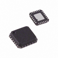
ADF4360-9BCPZ Analog Devices Inc, ADF4360-9BCPZ Datasheet - Page 12

ADF4360-9BCPZ
Manufacturer Part Number
ADF4360-9BCPZ
Description
Synthesizer And VCO
Manufacturer
Analog Devices Inc
Type
Fanout Distribution, Integer N Synthesizer (RF)r
Datasheet
1.ADF4360-9BCPZRL7.pdf
(24 pages)
Specifications of ADF4360-9BCPZ
Pll
Yes
Input
CMOS
Output
Clock
Number Of Circuits
1
Ratio - Input:output
1:2
Differential - Input:output
No/No
Frequency - Max
400MHz
Divider/multiplier
Yes/No
Voltage - Supply
3 V ~ 3.6 V
Operating Temperature
-40°C ~ 85°C
Mounting Type
Surface Mount
Package / Case
24-LFCSP
Frequency-max
400MHz
Number Of Elements
1
Supply Current
5mA
Pll Input Freq (min)
10MHz
Pll Input Freq (max)
250MHz
Operating Supply Voltage (typ)
3.3V
Operating Temp Range
-40C to 85C
Package Type
LFCSP EP
Output Frequency Range
1.1 to 400MHz
Operating Supply Voltage (min)
3V
Operating Supply Voltage (max)
3.6V
Operating Temperature Classification
Industrial
Pin Count
24
Lead Free Status / RoHS Status
Lead free / RoHS Compliant
Lead Free Status / RoHS Status
Lead free / RoHS Compliant
Available stocks
Company
Part Number
Manufacturer
Quantity
Price
Part Number:
ADF4360-9BCPZ
Manufacturer:
ADI/亚德诺
Quantity:
20 000
Company:
Part Number:
ADF4360-9BCPZRL7
Manufacturer:
Maxim
Quantity:
618
ADF4360-9
OUTPUT STAGE
The RF
connected to the collectors of an NPN differential pair driven
by buffered outputs of the VCO, as shown in Figure 19. To
allow the user to optimize the power dissipation vs. the output
power requirements, the tail current of the differential pair is
programmable via Bit PL1 and Bit PL2 in the control latch.
Four current levels can be set: 3.5 mA, 5 mA, 7.5 mA, and 11 mA.
These levels give output power levels of −9 dBm, −6 dBm,
−3 dBm, and 0 dBm, respectively, using the correct shunt inductor
to V
outputs can be combined in a 1 + 1:1 transformer or a 180°
microstrip coupler (see the Output Matching section).
Another feature of the ADF4360 family is that the supply
current to the RF output stage is shut down until the part
achieves lock, as measured by the digital lock detect circuitry.
This is enabled by the mute-till-lock detect (MTLD) bit in the
control latch.
DIVOUT STAGE
The output multiplexer on the ADF4360 family allows the user
to access various internal points on the chip. The state of DIVOUT
is controlled by D3, D2, and D1 in the control latch. The full
truth table is shown in Figure 23. Figure 20 shows the DIVOUT
section in block diagram form.
DD
and ac coupling into a 50 Ω load. Alternatively, both
OUT
A and RF
VCO
OUT
Figure 19. RF Output Stage
BUFFER
B pins of the ADF4360 family are
RF
OUT
A
RF
OUT
B
Rev. A | Page 12 of 24
The primary use of this pin is to derive the lower frequencies
from the VCO by programming various divider values to the
auxiliary A divider. Values ranging from 2 to 31 are possible.
The duty cycle of this output is 1/A times 100%, with the logic
high pulse width equal to the inverse of the VCO frequency.
That is,
See Figure 21 for a graphical description. By selecting the
divide-by-2 function, this divided down frequency can in turn
be divided by 2 again. This provides a 50% duty cycle in contrast to
the A counter output, which may be more suitable for some
applications (see Figure 21).
A COUNTER/2 OUTPUT
R COUNTER OUTPUT
N COUNTER OUTPUT
A COUNTER OUTPUT
f
f
f
VCO
VCO
VCO
Pulse Width [seconds] = 1/f
/A (A = 4)
/2A (A = 4)
Figure 21. DIVOUT Waveforms
Figure 20. DIVOUT Circuit
MUX
VCO
(Frequency [Hz])
CONTROL
DGND
DV
DD
DIVOUT


