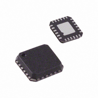
ADF4360-9BCPZ Analog Devices Inc, ADF4360-9BCPZ Datasheet - Page 4

ADF4360-9BCPZ
Manufacturer Part Number
ADF4360-9BCPZ
Description
Synthesizer And VCO
Manufacturer
Analog Devices Inc
Type
Fanout Distribution, Integer N Synthesizer (RF)r
Datasheet
1.ADF4360-9BCPZRL7.pdf
(24 pages)
Specifications of ADF4360-9BCPZ
Pll
Yes
Input
CMOS
Output
Clock
Number Of Circuits
1
Ratio - Input:output
1:2
Differential - Input:output
No/No
Frequency - Max
400MHz
Divider/multiplier
Yes/No
Voltage - Supply
3 V ~ 3.6 V
Operating Temperature
-40°C ~ 85°C
Mounting Type
Surface Mount
Package / Case
24-LFCSP
Frequency-max
400MHz
Number Of Elements
1
Supply Current
5mA
Pll Input Freq (min)
10MHz
Pll Input Freq (max)
250MHz
Operating Supply Voltage (typ)
3.3V
Operating Temp Range
-40C to 85C
Package Type
LFCSP EP
Output Frequency Range
1.1 to 400MHz
Operating Supply Voltage (min)
3V
Operating Supply Voltage (max)
3.6V
Operating Temperature Classification
Industrial
Pin Count
24
Lead Free Status / RoHS Status
Lead free / RoHS Compliant
Lead Free Status / RoHS Status
Lead free / RoHS Compliant
Available stocks
Company
Part Number
Manufacturer
Quantity
Price
Part Number:
ADF4360-9BCPZ
Manufacturer:
ADI/亚德诺
Quantity:
20 000
Company:
Part Number:
ADF4360-9BCPZRL7
Manufacturer:
Maxim
Quantity:
618
ADF4360-9
Parameter
VCO NOISE CHARACTERISTICS
DIVOUT CHARACTERISTICS
1
2
3
4
5
6
7
8
9
10
11
12
13
Operating temperature range is −40°C to +85°C.
Guaranteed by design. Sample tested to ensure compliance.
I
T
Unless otherwise stated, these characteristics are guaranteed for VCO core power = 5 mA. L1, L2 = 270 nH, 470 Ω resistors to GND in parallel with L1, L2.
Jumping from 90 MHz to 108 MHz. PFD frequency = 200 kHz; loop bandwidth = 10 kHz.
For more detail on using tuned loads, see the Output Matching section.
Using 50 Ω resistors to V
The noise of the VCO is measured in open-loop conditions. L1, L2 = 56 nH.
CP
The phase noise is measured with the EVAL-ADF4360-9EBZ1 evaluation board and the Agilent E5052A signal source analyzer.
f
VCO and subtracting 20logN (where N is the N divider value) and 10logf
The jitter is measured with the EVAL-ADF4360-9EBZ1 evaluation board and the Agilent E5052A signal source analyzer. A low noise TCXO provides the REF
synthesizer, and the jitter is measured over the instrument’s jitter measurement bandwidth. f
noted.
The spurious signals are measured with the EVAL-ADF4360-9EBZ1 evaluation board and the Agilent E5052A signal source analyzer. The spectrum analyzer provides
the REF
A
REFIN
Frequency Pushing (Open Loop)
Frequency Pulling (Open Loop)
Harmonic Content (Second)
Harmonic Content (Third)
Output Power
Output Power
Output Power Variation
VCO Tuning Range
VCO Phase Noise Performance
Normalized In-Band Phase Noise
In-Band Phase Noise
RMS Integrated Jitter
Spurious Signals Due to PFD Frequency
Integrated Jitter Performance
(Integrated from 100 Hz to 1 GHz)
DIVOUT Duty Cycle
= 25°C; AV
is internally modified to maintain constant loop gain over the frequency range.
DIVOUT = 180 MHz
DIVOUT = 95 MHz
DIVOUT = 80 MHz
DIVOUT = 52 MHz
DIVOUT = 45 MHz
DIVOUT = 10 MHz
A Output
A/2 Output
= 10 MHz; f
IN
for the synthesizer; f
DD
= DV
PFD
5, 7
5, 8
= 1 MHz; N = 360; loop B/W = 40 kHz. The normalized phase noise floor is estimated by measuring the in-band phase noise at the output of the
DD
= V
VCO
VCO
10, 11
12
into a 50 Ω load.
= 3.3 V.
REFIN
12
= 10 MHz @ 0 dBm. f
9,10
10, 11
13
REFIN
B Version
0.24
10
−16
−21
−9/0
−14/−9
±3
1.25/2.5
−91
−117
−139
−140
−147
−218
−110
1.4
−75
1.4
1.4
1.4
1.4
1.4
1.6
1/A × 100
50
= 10 MHz; f
PFD
PFD
Unit
MHz/V typ
Hz typ
dBc typ
dBc typ
dBm typ
dBm typ
dB typ
V min/V max
dBc/Hz typ
dBc/Hz typ
dBc/Hz typ
dBc/Hz typ
dBc/Hz typ
dBc/Hz typ
dBc/Hz typ
ps typ
dBc typ
ps rms
ps rms
ps rms
ps rms
ps rms
ps rms
% typ
% typ
Rev. A | Page 4 of 24
= 1 MHz; N = 360; loop BW = 40 kHz.
. PN
SYNTH
= PN
TOT
− 10logf
REFIN
= 10 MHz; f
PFD
Divide-by-A selected
Divide-by-A/2 selected
Conditions/Comments
Into 2.00 VSWR load
Using tuned load, programmable in 3 dB steps;
see Figure 35
Using 50 Ω resistors to V
3 dB steps; see Figure 33
@ 10 kHz offset from carrier
@ 100 kHz offset from carrier
@ 1 MHz offset from carrier
@ 3 MHz offset from carrier
@ 10 MHz offset from carrier
@ 1 kHz offset from carrier
Measured at RF
VCO frequency = 320 MHz to 380 MHz
A = 2, A output selected
A = 2, A/2 output selected
A = 2, A/2 output selected
A = 3, A/2 output selected (VCO = 312 MHz,
PFD = 1.6 MHz)
A = 4, A/2 output selected
A = 18, A/2 output selected (VCO = 360 MHz,
PFD = 1.6 MHz)
− 20logN.
PFD
= 1 MHz; N = 360; loop BW = 40 kHz, unless otherwise
OUT
A
VCO
, programmable in
IN
for the


