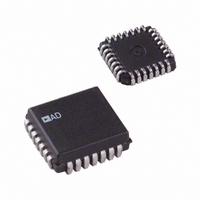
ADG406BPZ-REEL Analog Devices Inc, ADG406BPZ-REEL Datasheet

ADG406BPZ-REEL
Specifications of ADG406BPZ-REEL
Available stocks
Related parts for ADG406BPZ-REEL
ADG406BPZ-REEL Summary of contents
Page 1
FEATURES 44 V supply maximum ratings analog signal range SS DD Low on resistance (80 Ω maximum) Low power Fast switching t < 160 < 150 ns OFF Break-before-make switching action APPLICATIONS Audio and ...
Page 2
ADG406/ADG407/ADG426 TABLE OF CONTENTS Features .............................................................................................. 1 Applications ....................................................................................... 1 Product Highlights ........................................................................... 1 Functional Block Diagrams ............................................................. 1 Revision History ............................................................................... 2 General Description ......................................................................... 3 Specifications ..................................................................................... 4 Dual Supply ................................................................................... 4 Single Supply ................................................................................. 6 REVISION HISTORY ...
Page 3
GENERAL DESCRIPTION The ADG406, ADG407, and ADG426 are monolithic CMOS analog multiplexers. The ADG406 and ADG426 switch one of sixteen inputs to a common output as determined by the 4-bit binary address lines: A0, A1, A2, and A3. The ADG426 ...
Page 4
ADG406/ADG407/ADG426 SPECIFICATIONS DUAL SUPPLY V = +15 V ± 10 −15 V ± 10%, GND = 0 V, unless otherwise noted Table 1. 1 Parameter ANALOG SWITCH Analog Signal Range Match ON LEAKAGE ...
Page 5
Parameter +25°C POWER REQUIREMENTS 100 DD 200 Temperature ranges is −40°C to +85°C. 2 Guaranteed by design, not subject to production test. −40°C to +85°C Unit Test Conditions/Comments V = +16.5 ...
Page 6
ADG406/ADG407/ADG426 SINGLE SUPPLY V = +12 V ± 10 GND = 0 V, unless otherwise noted Table 2. Parameter 1 +25°C ANALOG SWITCH Analog Signal Range 125 LEAKAGE CURRENTS Source Off ...
Page 7
ADG426 TIMING DIAGRAMS A0, A1, A2, (A3 Figure 4. Timing Sequence for Latching the Switch Address and Enable Inputs Figure 4 shows the timing sequence for latching the ...
Page 8
ADG406/ADG407/ADG426 ABSOLUTE MAXIMUM RATINGS T = 25°C unless otherwise noted. A Table 3. Parameter Rating GND −0 + GND +0 − ...
Page 9
PIN CONFIGURATIONS AND FUNCTION DESCRIPTIONS S16 4 25 S15 24 5 ADG406 S14 23 6 TOP VIEW S13 22 7 (Not to Scale) S12 21 8 S11 9 20 S10 ...
Page 10
ADG406/ADG407/ADG426 S8B 4 25 S7B 5 24 ADG407 S6B 6 23 TOP VIEW S5B 22 7 (Not to Scale) S4B 21 8 S3B 9 20 S2B 10 19 S1B 11 ...
Page 11
Table 8. Pin Function Descriptions Pin No. Mnemonic Description 1 V Most Positive Power Supply Potential Connect Active Low Logic Input. When this pin is low, all switches are open, and address and enable ...
Page 12
ADG406/ADG407/ADG426 TYPICAL PERFORMANCE CHARACTERISTICS 150 120 +10V –10V +15V –15V SS 0 –15 –10 – ( Figure 11. ...
Page 13
0.1 100 1k 10k 100k FREQUENCY (Hz) Figure 17. Positive Supply Current vs. Switching Frequency 160 t ON 140 t TRANSITION 120 100 ...
Page 14
ADG406/ADG407/ADG426 140 120 100 100 1k 10k 100k FREQUENCY (Hz) Figure 23. Off Isolation vs. Frequency 140 V = +15V –15V SS 120 100 10M 100 Rev Page ...
Page 15
TEST CIRCUITS V1 Figure 25. On Resistance (OFF S16 Figure 26. I (Off) ...
Page 16
ADG406/ADG407/ADG426 THRU S16 A1 ADG426 A0 2. GND V 50Ω SIMILAR CONNECTION FOR ADG406/ADG407 THRU S16 A1 ADG426 ...
Page 17
ADG426 GND WR 1 SIMILAR CONNECTION FOR ADG406/ADG407 S16 A1 1 ...
Page 18
ADG406/ADG407/ADG426 TERMINOLOGY V DD Most positive power supply potential Most negative power supply potential in dual supplies. In single supply applications, it may be connected to ground. GND Ground (0 V) reference Ohmic resistance between the ...
Page 19
OUTLINE DIMENSIONS 28 1 0.250 (6.35) MAX 0.200 (5.08) 0.115 (2.92) 0.022 (0.56) 0.014 (0.36) 0.048 (1.22) 0.042 (1.07) 4 0.048 (1.22) 5 0.042 (1.07) IDENTIFIER TOP VIEW (PINS DOWN 0.456 (11.582) 0.450 (11.430) 0.495 (12.57) 0.485 (12.32) ...
Page 20
... ADG406BNZ −40°C to +85°C ADG406BP −40°C to +85°C ADG406BP-REEL −40°C to +85°C ADG406BPZ −40°C to +85°C ADG406BPZ-REEL −40°C to +85°C ADG407BN −40°C to +85°C ADG407BNZ −40°C to +85°C ADG407BP −40°C to +85°C ADG407BP-REEL − ...


