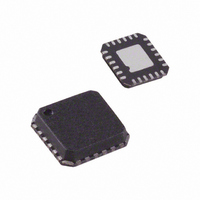
ADL5371ACPZ-R7 Analog Devices Inc, ADL5371ACPZ-R7 Datasheet

ADL5371ACPZ-R7
Specifications of ADL5371ACPZ-R7
Available stocks
Related parts for ADL5371ACPZ-R7
ADL5371ACPZ-R7 Summary of contents
Page 1
FEATURES Output frequency range: 500 MHz to 1500 MHz Modulation bandwidth: >500 MHz (3 dB output compression: 14.4 dBm @ 900 MHz Noise floor: −158.6 dBm/Hz @ 915 MHz Sideband suppression: −55 dBc @ 900 MHz Carrier feedthrough: ...
Page 2
ADL5371 TABLE OF CONTENTS Features .............................................................................................. 1 Applications....................................................................................... 1 Functional Block Diagram .............................................................. 1 General Description ......................................................................... 1 Revision History ............................................................................... 2 Specifications..................................................................................... 3 Absolute Maximum Ratings............................................................ 4 ESD Caution.................................................................................. 4 Pin Configuration and Function Descriptions............................. 5 Typical Performance Characteristics ...
Page 3
SPECIFICATIONS 25° dBm single-ended; baseband I/Q amplitude = 1.4 V p-p differential sine waves in quadrature with a 500 bias; baseband I/Q frequency ( ...
Page 4
ADL5371 ABSOLUTE MAXIMUM RATINGS Table 2. Parameter Supply Voltage VPOS IBBP, IBBN, QBBP, QBBN LOIP and LOIN Internal Power Dissipation θ (Exposed Paddle Soldered Down) JA Maximum Junction Temperature Operating Temperature Range Storage Temperature Range Stresses above those listed under ...
Page 5
PIN CONFIGURATION AND FUNCTION DESCRIPTIONS Table 3. Pin Function Descriptions Pin No. Mnemonic Description 1, 2 COM1 Input Common Pins. Connect to ground plane via a low impedance path COM2 Input Common Pins. Connect to ground plane via ...
Page 6
ADL5371 TYPICAL PERFORMANCE CHARACTERISTICS 25° dBm single-ended; baseband I/Q amplitude = 1.4 V p-p differential sine waves in quadrature with a 500 bias; baseband I/Q frequency (f ...
Page 7
LO FREQUENCY (MHz) Figure 9. Return Loss (S11) of LOIP 0 –10 –20 – –40° +25° –40 ...
Page 8
ADL5371 –20 –30 THIRD-ORDER –40 THIRD-ORDER T = +85° +25°C A –50 –60 SECOND-ORDER T = +25°C A –70 SECOND-ORDER T = +85°C A –80 500 600 700 800 900 1000 1100 1200 1300 1400 1500 LO ...
Page 9
NOISE AT 20MHz OFFSET (dBm/Hz) Figure 21. 20 MHz Offset Noise Floor Distribution at f (I/Q Amplitude = 0 mV p-p with 500 mV dc Bias 915MHz LO = 915 MHz LO ...
Page 10
ADL5371 THEORY OF OPERATION CIRCUIT DESCRIPTION Overview The ADL5371 can be divided into five circuit blocks: the LO interface, the baseband voltage-to-current (V-to-I) converter, the mixers, the differential-to-single-ended (D-to-S) converter, and the bias circuit. A detailed block diagram of the ...
Page 11
BASIC CONNECTIONS Figure 23 shows the basic connections for the ADL5371. QBBP QBBN IBBN IBBP COM1 1 18 COM1 F-MOD VPS1 3 16 VPS1 4 15 VPS1 5 14 VPS1 EXPOSED PADDLE 6 13 C12 0.1µF GND ...
Page 12
ADL5371 OPTIMIZATION The carrier feedthrough and sideband suppression performance of the ADL5371 can be improved by using optimization techniques. Carrier Feedthrough Nulling Carrier feedthrough results from minute dc offsets that occur between each of the differential baseband inputs ...
Page 13
APPLICATIONS INFORMATION DAC MODULATOR INTERFACING The ADL5371 is designed to interface with minimal components to members of the Analog Devices family of DACs. These DACs feature an output current swing from mA, and the interface described in ...
Page 14
ADL5371 Figure 30 shows an example of a third-order elliptical filter with frequency of 3 MHz. Matching input and output impedances makes the filter design easier, so the shunt resistor chosen is 100 Ω, producing an ac ...
Page 15
LO GENERATION USING PLLS Analog Devices has a line of PLLs that can be used for generating the LO signal. Table 4 lists the PLLs together with their maximum frequency and phase noise performance. Table 4. ADI PLL Selection Table ...
Page 16
ADL5371 EVALUATION BOARD Populated RoHS-compliant evaluation boards are available for evaluation of the ADL5371. The ADL5371 package has an exposed paddle on the underside. This exposed paddle must be soldered to the board (see the Power Supply and Grounding section). ...
Page 17
CHARACTERIZATION SETUP AEROFLEX 250kHz TO 6GHz SIGNAL GENERATOR AGILENT 34401A MULTIMETER VPOS +5V AGILENT E3631A POWER SUPPLY 6V – + The primary setup used to characterize the ADL5371 is shown in Figure 36. This setup was used to evaluate the ...
Page 18
ADL5371 TEKTRONIX AFG3252 DUAL FUNCTION ARBITRARY FUNCTION GENERATOR 0° AGILENT E3631A POWER SUPPLY 6V VPOS +5V – +5V VPOS +5V AGILENT E3631A POWER SUPPLY 6V ±25V – COM VCM = 0.5V AGILENT 34401A MULTIMETER Figure 37. ...
Page 19
... OUTLINE DIMENSIONS PIN 1 INDICATOR 1.00 0.85 0.80 SEATING PLANE ORDERING GUIDE Model Temperature Range 1 ADL5371ACPZ-R2 –40°C to +85°C ADL5371ACPZ-R7 1 –40°C to +85°C 1 ADL5371ACPZ-WP –40°C to +85°C 1 ADL5371-EVALZ Pb-free part. 4.00 BSC SQ 0.60 MAX 0.50 BSC TOP 3.75 VIEW BSC SQ 0 ...
Page 20
ADL5371 NOTES ©2007 Analog Devices, Inc. All rights reserved. Trademarks and registered trademarks are the property of their respective owners. D06510-0-1/07(0) T Rev Page ...


