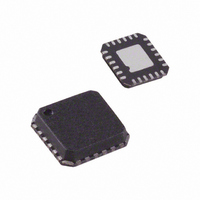
ADL5371ACPZ-R7 Analog Devices Inc, ADL5371ACPZ-R7 Datasheet - Page 10

ADL5371ACPZ-R7
Manufacturer Part Number
ADL5371ACPZ-R7
Description
IC,RF Modulator,LLCC,24PIN,PLASTIC
Manufacturer
Analog Devices Inc
Datasheet
1.ADL5371ACPZ-R7.pdf
(20 pages)
Specifications of ADL5371ACPZ-R7
Design Resources
Interfacing ADL5371 to AD9779A Dual-Channel, 1 GSPS High Speed DAC (CN0017)
Function
Modulator
Lo Frequency
500MHz ~ 1.5GHz
Rf Frequency
500MHz ~ 1.5GHz
P1db
14.4dBm
Noise Floor
-158.6dBm/Hz
Output Power
7.6dBm
Current - Supply
200mA
Voltage - Supply
4.75 V ~ 5.25 V
Test Frequency
900MHz
Package / Case
24-VFQFN, 24-CSP Exposed Pad
Lead Free Status / RoHS Status
Lead free / RoHS Compliant
Other names
ADL5371ACPZ-R7TR
Available stocks
Company
Part Number
Manufacturer
Quantity
Price
Company:
Part Number:
ADL5371ACPZ-R7
Manufacturer:
Bussmann
Quantity:
500
Part Number:
ADL5371ACPZ-R7
Manufacturer:
ADI/亚德诺
Quantity:
20 000
ADL5371
THEORY OF OPERATION
CIRCUIT DESCRIPTION
Overview
The ADL5371 can be divided into five circuit blocks: the LO
interface, the baseband voltage-to-current (V-to-I) converter,
the mixers, the differential-to-single-ended (D-to-S) converter,
and the bias circuit. A detailed block diagram of the device is
shown in Figure 22.
The LO interface generates two LO signals in quadrature. These
signals are used to drive the mixers. The I/Q baseband input
signals are converted to currents by the V-to-I stages, which
then drive the two mixers. The outputs of these mixers combine
to feed the output balun, which provides a single-ended output
interface. The bias cell generates a reference current for the
V-to-I stage.
LO Interface
The LO interface consists of a polyphase quadrature splitter
followed by a limiting amplifier. The LO input impedance is set
by the polyphase. The LO can be driven either single-ended or
differentially. When driven single-ended, the LOIN pin should
be ac-grounded via a capacitor. Each quadrature LO signal then
passes through a limiting amplifier that provides the mixer with
a limited drive signal.
QBBN
QBBP
IBBN
LOIN
IBBP
LOIP
Figure 22. Block Diagram
SPLITTER
PHASE
Σ
OUT
Rev. 0 | Page 10 of 20
V-to-I Converter
The differential baseband inputs (QBBP, QBBN, IBBN, and
IBBP) consist of the bases of PNP transistors, which present a
high impedance. The voltages applied to these pins drive the
V-to-I stage that converts baseband voltages into currents. The
differential output currents of the V-to-I stages feed each of
their respective Gilbert-cell mixers. The dc common-mode
voltage at the baseband inputs sets the currents in the two mixer
cores. Varying the baseband common-mode voltage varies the
current in the mixer and affects overall modulator performance.
The recommended dc voltage for the baseband common-mode
voltage is 500 mV dc.
Mixers
The ADL5371 has two double-balanced mixers: one for the
in-phase channel (I channel) and one for the quadrature
channel (Q channel). Both mixers are based on the Gilbert-cell
design of four cross-connected transistors. The output currents
from the two mixers sum together into an on-chip balun, which
converts the differential signal to single-ended.
D-to-S Stage
The output D-to-S stage consists of an on-chip balun that
converts the differential signal to a single-ended signal. The
balun presents high impedance to the output (VOUT).
Therefore, a matching network may be needed at the output for
optimal power transfer.
Bias Circuit
An on-chip band gap reference circuit is used to generate a
proportional-to-absolute temperature (PTAT) reference current
for the V-to-I stage.


