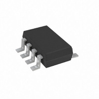
ADM1172-1AUJZ-RL7 Analog Devices Inc, ADM1172-1AUJZ-RL7 Datasheet

ADM1172-1AUJZ-RL7
Specifications of ADM1172-1AUJZ-RL7
Available stocks
Related parts for ADM1172-1AUJZ-RL7
ADM1172-1AUJZ-RL7 Summary of contents
Page 1
... V to 16.5 V Hot Swap Controller with Power-Fail Comparator GENERAL DESCRIPTION The ADM1172 is a hot swap controller that safely enables a printed circuit board to be removed and inserted to a live backplane. This is achieved using an external N-channel power MOSFET with a current control loop that monitors the load current through a sense resistor ...
Page 2
... ADM1172 TABLE OF CONTENTS Features .............................................................................................. 1 Applications....................................................................................... 1 General Description ......................................................................... 1 Functional Block Diagram .............................................................. 1 Revision History ............................................................................... 2 Specifications..................................................................................... 3 Absolute Maximum Ratings............................................................ 4 Thermal Characteristics .............................................................. 4 ESD Caution.................................................................................. 4 Pin Configurations and Function Descriptions ........................... 5 Typical Performance Characteristics ............................................. 6 Theory of Operation ...................................................................... 12 Overview...................................................................................... 12 REVISION HISTORY 7/06—Revision 0: Initial Version UVLO........................................................................................... 12 ON (ON- CLR ) Pin..................................................................... 12 GATE ...
Page 3
... TIMERDN 100 μA V 1.22 1.3 1.38 V TIMERH V 0.15 0.2 0.25 V TIMERL 0.58 0.6 0. − μA −5 μA 0 μs 40 μs 40 μs Rev Page ADM1172 Conditions V rising CC ON rising – SENSE V − 3.0 V GATE − 3.3 V GATE − GATE − GATE ...
Page 4
... ADM1172 ABSOLUTE MAXIMUM RATINGS Table 2. Parameter V Pin CC SENSE Pin V − SENSE CC TIMER Pin ON (ON-CLR ) Pin PFI Pin PFO Pin GATE Pin Storage Temperature Range Operating Temperature Range Lead Temperature (10 sec) Junction Temperature ESD CAUTION ESD (electrostatic discharge) sensitive device. Electrostatic charges as high as 4000 V readily accumulate on the human body and test equipment and can discharge without detection ...
Page 5
... Input Pin. The ON (ON-CLR) pin is an input to a comparator that has a low-to-high threshold of 1.3 V with 80 mV hysteresis and a glitch filter. The ADM1172 is reset when the ON (ON-CLR) pin is low. When the ON (ON-Error!) pin is high, the ADM1172 is enabled. A rising edge on this pin has the added function of clearing a fault and restarting the device on the latched off model, the ADM1172-2. ...
Page 6
... ADM1172 TYPICAL PERFORMANCE CHARACTERISTICS 0.50 0.45 0.40 0.35 0.30 0.25 0.20 0.15 0.10 0. SUPPLY VOLTAGE (V) Figure 4. Supply Current vs. Supply Voltage (GATE Off) 0.8 0.7 0.6 0.5 0.4 0.3 0.2 0 SUPPLY VOLTAGE (V) Figure 5. Supply Current vs. Supply Voltage (GATE On) 1.0 0.9 0 12V 0 ...
Page 7
... Figure 14. I – 20 –30 –40 –50 –60 –70 –80 –90 –100 1 – Figure 15. I Rev Page ADM1172 – 100 125 TEMPERATURE (°C) Figure 13. I (In Initial Cycle) vs. Temperature TIMERUP T = 25° SUPPLY VOLTAGE (V) (During Cct Breaker Delay) vs. Supply Voltage ...
Page 8
... ADM1172 3 25°C A 2.8 2.6 2.4 2.2 2.0 1.8 1.6 1.4 1.2 1 SUPPLY VOLTAGE (V) Figure 16. I (In Cool-Off Cycle) vs. Supply Voltage TIMERDN 3 2.8 2.6 2.4 2.2 2.0 1.8 1.6 1.4 1.2 1.0 –50 – TEMPERATURE (°C) Figure 17. I (In Cool-Off Cycle) vs. Temperature TIMERDN 1 ...
Page 9
... Figure 24. t vs. Supply Voltage OFF(ONLOW – 125 150 – Rev Page ADM1172 V = 15V 12V – 100 125 TEMPERATURE (°C) Figure 25. t vs. Temperature OFF(ONLOW SUPPLY VOLTAGE (V) Figure 26. Cct Breaker Voltage vs. Supply Voltage – 100 125 TEMPERATURE (°C) Figure 27. Cct Breaker Voltage vs. Temperature 150 ...
Page 10
... ADM1172 SUPPLY VOLTAGE (V) Figure 28. GATE Current (Down) vs. Supply Voltage –8 –9 –10 –11 –12 –13 – SUPPLY VOLTAGE (V) Figure 29. GATE Current (Up) vs. Supply Voltage –11.0 –11.2 –11.4 –11.6 –11 –12 –12 –12 15V –12.6 CC –12.8 –13.0 –50 – TEMPERATURE (°C) Figure 30. GATE Current (up) vs. Temperature ...
Page 11
... V = 15V CC 0.06 0.04 0. 300µA 0 –50 150 Figure 36. PFO Output Low Voltage vs. Temperature 100 μA 700 600 500 400 300 200 100 I = 500µA 0 150 –0.1 Rev Page ADM1172 15V 12V 100µ 100 TEMPERATURE (° 15V 0.1 0.3 ...
Page 12
... The ADM1172 can reside either on the backplane or on the removable board. OVERVIEW The ADM1172 operates over a supply range the supply voltage is coming up, an undervoltage lockout circuit checks if sufficient supply voltage is present for proper operation. During this period, the FET is held off by the GATE pin being held to GND ...
Page 13
... ADM1172. A capacitor controls the initial power on reset time and the amount of time an overcurrent condition lasts before the FET shuts down. On the ADM1172-1, the timer pin also controls the time between auto retry pulses. There are pull-up and pull-down currents internally available to control the timer functions ...
Page 14
... Figure 40 for details). The period of this cycle is determined by the timer capacitor at a duty cycle of 3.8% on and 96.2% off. The ADM1172-2 model has a latch off system whereby when a pin current fault is detected, the GATE is switched off after a time ...
Page 15
... OUTLINE DIMENSIONS INDICATOR 0.10 MAX ORDERING GUIDE Model Temperature Range 1 ADM1172-1AUJZ-RL7 −40°C to +85°C 1 ADM1172-2AUJZ-RL7 −40°C to +85° Pb-free part. 2.90 BSC 1.60 BSC 2.80 BSC PIN 1 0.65 BSC 1.95 * 0.90 BSC 0.87 0.84 * 1.00 MAX 0.20 0.08 0.38 SEATING 0 ...
Page 16
... ADM1172 NOTES ©2006 Analog Devices, Inc. All rights reserved. Trademarks and registered trademarks are the property of their respective owners. D05126-0-7/06(0) Rev Page ...


